05.31.16
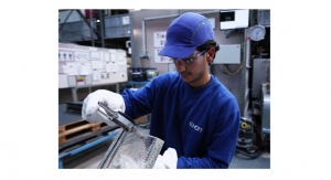
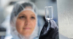
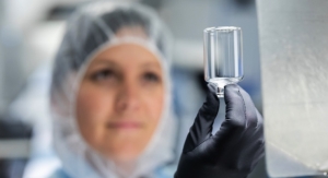
SCHOTT’s glass wafers and substrates serve as key materials in the fields of IC packaging, radio frequency (RF) components, and micro-electromechanical systems (MEMS). SCHOTT is presenting its industry-leading thin and ultra-thin glass wafers, and sheets for semiconductors and optoelectronics, at the Electronic Components and Technology Conference (ECTC) from May 31-June 6 in Las Vegas.
SCHOTT’s broad portfolio of glass wafers and substrates is known for its chemical and thermomechanical properties and surface qualities. The wafers and substrates are available in different sizes (wafer diameters up to 12 inches; sheet sizes up to 510 x 510 mm2) and thicknesses (from 1.1 mm down to ultra-thin 25 µm). Additionally, SCHOTT offers extensive application support in the field of handling technologies and formation of glass wafers with through glass vias (TGV), which cover a wide spectrum of feature sizes.
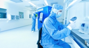
“With these technologies, SCHOTT can support the emerging ‘More-than-Moore’ trends throughout the electronics industry,” said Dr. Rüdiger Sprengard, director new business Ultra-Thin Glass at SCHOTT AG. “Ultra-thin glass wafers and substrates are enabling consumer electronics to be even thinner, and help make possible the high-performance computing necessary for applications like self-driving cars.”
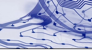
SCHOTT recently expanded its wafer portfolio with FOTURAN II, a photo-structurable glass that is significantly more advanced in quality, such as material homogeneity, than its 30-year-old predecessor. The material’s unique properties enable high aspect ratio and small feature sizes in RF components and MEMS systems. FOTURAN II wafers can be structured and processed in three steps: UV-exposure (with standard lithography equipment, but without the use of photo-resist), tempering, and etching; additional ceramization is an option when higher temperature stability is required.
“Superior materials, like ultra-thin glass wafers, give engineers the ability to pack more power into smaller forms,” said Sprengard. “The next innovations in semiconductor and optoelectronics technologies, such as MEMS and driverless car components, are made possible with specialty glass.”
SCHOTT’s broad portfolio of glass wafers and substrates is known for its chemical and thermomechanical properties and surface qualities. The wafers and substrates are available in different sizes (wafer diameters up to 12 inches; sheet sizes up to 510 x 510 mm2) and thicknesses (from 1.1 mm down to ultra-thin 25 µm). Additionally, SCHOTT offers extensive application support in the field of handling technologies and formation of glass wafers with through glass vias (TGV), which cover a wide spectrum of feature sizes.
“With these technologies, SCHOTT can support the emerging ‘More-than-Moore’ trends throughout the electronics industry,” said Dr. Rüdiger Sprengard, director new business Ultra-Thin Glass at SCHOTT AG. “Ultra-thin glass wafers and substrates are enabling consumer electronics to be even thinner, and help make possible the high-performance computing necessary for applications like self-driving cars.”
SCHOTT recently expanded its wafer portfolio with FOTURAN II, a photo-structurable glass that is significantly more advanced in quality, such as material homogeneity, than its 30-year-old predecessor. The material’s unique properties enable high aspect ratio and small feature sizes in RF components and MEMS systems. FOTURAN II wafers can be structured and processed in three steps: UV-exposure (with standard lithography equipment, but without the use of photo-resist), tempering, and etching; additional ceramization is an option when higher temperature stability is required.
“Superior materials, like ultra-thin glass wafers, give engineers the ability to pack more power into smaller forms,” said Sprengard. “The next innovations in semiconductor and optoelectronics technologies, such as MEMS and driverless car components, are made possible with specialty glass.”