03.15.17
Researchers have long sought electrically conductive materials for economical energy-storage devices. Two-dimensional (2D) ceramics called MXenes are contenders. Unlike most 2D ceramics, MXenes have inherently good conductivity because they are molecular sheets made from the carbides and nitrides of transition metals like titanium.
MXenes were co-discovered by Michael Naguib, now a Wigner Fellow at the Department of Energy’s Oak Ridge National Laboratory (ORNL), while pursuing his PhD at Drexel University in 2011. MXene layers can be combined to engineer ultrathin electronics, sensors, batteries, supercapacitors and catalysts. About 20 MXenes have since been reported.
Recently, ORNL scientists using state-of-the-art scanning transmission electron microscopy, or STEM, provided the first direct evidence of the atomic-defect configurations in a titanium-carbide MXene synthesized at Drexel University. Published in ACS Nano, a journal of the American Chemical Society, the study coupled atomic-scale characterization and electrical property measurements with theory-based simulation.
“Using atomic-resolution scanning transmission electron microscopy imaging, we visualized defects and defects clusters in MXene that are very important for future nano electronic devices and catalytic applications,” said lead author Xiahan Sang of the Center for Nanophase Materials Sciences (CNMS), a DOE Office of Science User Facility at ORNL.
“Atomic-level defects can be engineered into materials to enable new functionalities,” said senior author Raymond Unocic of CNMS. “Understanding these defects is critical for advancing materials.”
Atomic imaging from different perspectives was the key to revealing MXene’s structure. When the sample is aligned with the electron beam within a STEM instrument, the viewer cannot tell how many sheets lie under the top layer. But simply tilt the sample, and differences readily appear.
MXenes are made from a three-dimensional (3D) bulk crystal called MAX (the “M” denotes a transition metal; “A,” an element, such as aluminum or silicon, from a specific chemical group; and “X,” either carbon or nitrogen). In the MAX lattice from which the MXene explored in this study emerged, three layers of titanium carbide are sandwiched between aluminum layers.
The Drexel researchers improved a technique developed in 2011 and altered in 2014 to synthesize MXene from the bulk MAX phase using acids. The improved method is called minimally intensive layer delamination, or MILD.
Etching creates defects—vacant spaces that emerge as titanium atoms are pulled from surfaces. “Defects” are actually good in many applications of materials. They can be introduced into a material and manipulated to enhance its useful catalytic, optical or electronic properties.
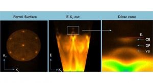
Moreover, the number of defects did not strongly affect MXene’s electrical conductivity. At CNMS, Ming-Wei Lin and Kai Xiao measured physical properties, including electrical conductivity, of various promising 2D materials. They found MXene was an order of magnitude less conductive than a perfect graphene sheet but two orders of magnitude more conductive than metallic molybdenum disulfide.
MXenes were co-discovered by Michael Naguib, now a Wigner Fellow at the Department of Energy’s Oak Ridge National Laboratory (ORNL), while pursuing his PhD at Drexel University in 2011. MXene layers can be combined to engineer ultrathin electronics, sensors, batteries, supercapacitors and catalysts. About 20 MXenes have since been reported.
Recently, ORNL scientists using state-of-the-art scanning transmission electron microscopy, or STEM, provided the first direct evidence of the atomic-defect configurations in a titanium-carbide MXene synthesized at Drexel University. Published in ACS Nano, a journal of the American Chemical Society, the study coupled atomic-scale characterization and electrical property measurements with theory-based simulation.
“Using atomic-resolution scanning transmission electron microscopy imaging, we visualized defects and defects clusters in MXene that are very important for future nano electronic devices and catalytic applications,” said lead author Xiahan Sang of the Center for Nanophase Materials Sciences (CNMS), a DOE Office of Science User Facility at ORNL.
“Atomic-level defects can be engineered into materials to enable new functionalities,” said senior author Raymond Unocic of CNMS. “Understanding these defects is critical for advancing materials.”
Atomic imaging from different perspectives was the key to revealing MXene’s structure. When the sample is aligned with the electron beam within a STEM instrument, the viewer cannot tell how many sheets lie under the top layer. But simply tilt the sample, and differences readily appear.
MXenes are made from a three-dimensional (3D) bulk crystal called MAX (the “M” denotes a transition metal; “A,” an element, such as aluminum or silicon, from a specific chemical group; and “X,” either carbon or nitrogen). In the MAX lattice from which the MXene explored in this study emerged, three layers of titanium carbide are sandwiched between aluminum layers.
The Drexel researchers improved a technique developed in 2011 and altered in 2014 to synthesize MXene from the bulk MAX phase using acids. The improved method is called minimally intensive layer delamination, or MILD.
Etching creates defects—vacant spaces that emerge as titanium atoms are pulled from surfaces. “Defects” are actually good in many applications of materials. They can be introduced into a material and manipulated to enhance its useful catalytic, optical or electronic properties.
Moreover, the number of defects did not strongly affect MXene’s electrical conductivity. At CNMS, Ming-Wei Lin and Kai Xiao measured physical properties, including electrical conductivity, of various promising 2D materials. They found MXene was an order of magnitude less conductive than a perfect graphene sheet but two orders of magnitude more conductive than metallic molybdenum disulfide.