12.07.17
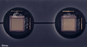
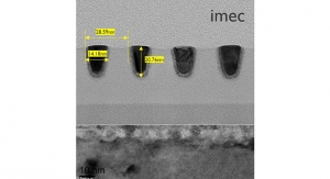
At this week’s 2017 International Electron Devices Meeting (IEDM), imec reports on multiple key process optimizations for vertically stacked gate-all-around (GAA) silicon nanowire transistors. The optimized CMOS process flow was then used to integrate, for the first time, the GAA nanowire transistors in a functional ring oscillator. This demonstrator shows the promise this technology holds for realizing the sub-5nm technology nodes.
Gate-all-around (GAA) MOSFETs based on vertically stacked horizontal nanowires or nanosheets are promising candidates to succeed FinFETs in sub-5nm technology nodes, thus extending today’s CMOS technology beyond its scaling limits. In very scaled standard cells where only one fin device is allowed, nanosheets provide more current per footprint than fins, and thus can drive higher capacitive loads.
As with every disruptive innovation, this new architecture demands for process optimizations. At IEDM, a team of researchers from imec and Applied Materials demonstrated multiple optimizations for the fabrication of stacked silicon nanowire and nanosheet FETs.
“GAA nanowire transistors are key in further CMOS scaling,” said Naoto Horiguchi, distinguished member of the technical staff at imec. “Earlier this year, we demonstrated standalone transistors and CMOS integration. Now the next step was taken with a full demonstrator, showing the enormous promise this technology holds for realizing the sub-7 nm technology nodes.”