03.02.18
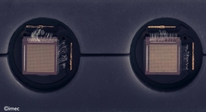
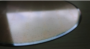
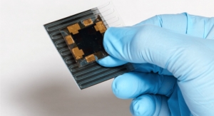
Imec and Cadence Design Systems, Inc. announced that its extensive, long-standing collaboration has resulted in the industry’s first 3nm test chip tapeout.
The tapeout project, geared toward advancing 3nm chip design, was completed using extreme ultraviolet (EUV) and 193 immersion (193i) lithography-oriented design rules and the Cadence Innovus Implementation System and Genus Synthesis Solution. Imec utilized a common industry 64-bit CPU for the test chip with a custom 3nm standard cell library and a TRIM metal flow, where the routing pitch was reduced to 21nm.
Together, Cadence and imec have enabled the 3nm implementation flow to be fully validated in preparation for next-generation design innovation.
“As process dimensions reduce to the 3nm node, interconnect variation becomes much more significant,” said An Steegen, EVP for semiconductor technology and systems at imec. “Our work on the test chip has enabled interconnect variation to be measured and improved and the 3nm manufacturing process to be validated. Also, the Cadence digital solutions offered everything needed for this 3nm implementation.”