06.18.18
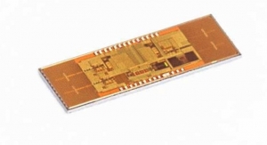
At this week’s 2018 Symposia on VLSI Technology and Circuits, imec demonstrates for the first time the possibility to fabricate state-of-the-art spin-orbit torque MRAM (SOT-MRAM) devices on 300mm wafers using CMOS compatible processes.
With an unlimited endurance (>5x10¹⁰), fast switching speed (210ps), and power consumption as low as 300pJ, the SOT-MRAM devices manufactured in a 300mm line achieve the same or better performance as lab devices. This next-generation MRAM technology targets replacement of L1/L2 SRAM cache memories in high-performance computing applications.
SOT-MRAM has recently emerged as a non-volatile memory technology that promises a high endurance and low-power, sub-ns switching speed. With these properties, it can potentially overcome the limitations of spin-transfer torque MRAM (STT-MRAM) for L1/L2 SRAM cache memory replacement. But so far, SOT-MRAM devices have only been demonstrated in the lab. Imec has now for the first time proven full-scale integration of SOT-MRAM device modules on 300mm wafers using CMOS-compatible processes.
At the core of the SOT-MRAM device is a magnetic tunnel junction in which a thin dielectric layer is sandwiched between a magnetic fixed layer and a magnetic free layer. Similar as for STT-MRAM operation, writing of the memory is performed by switching the magnetization of this free magnetic layer, by means of a current. In an SOT-MRAM device, switching of the free magnetic layer is done by injecting an in-plane current in an adjacent SOT layer – typically made of a heavy metal. Because of the current injection geometry, the read and write path are de-coupled, significantly improving the device endurance and read stability.
“STT-MRAM technology has a high potential to replace L3 cache memory in high-performance computing applications”, said Gouri Sankar Kar, distinguished member of technical staff at imec. “However, due to the challenging reliability and increased energy at sub-ns switching speeds, they are unsuitable to replace the faster L1/L2 SRAM cache memories. SOT-MRAM technology will help us to expand MRAM operation into the SRAM application domain. By moving this next-generation MRAM technology out of the lab, we have now demonstrated the maturity of the technology.”