David Savastano, Editor01.04.12
One of the key value propositions for the field of printed electronics is the ability to use printing processes to manufacture semiconductors. There have been some successes in this field, but mass commercialization has yet to emerge.
PST Sensors is poised to make a major breakthrough in this field. Led by directors Margit Harting and David Britton, who have been working on this technology as professors at the University of Cape Town (UCT), PST Sensors has developed and proven its technology to print silicon semiconductors at room temperature on any material, including paper, using conventional printing methods.
PST Sensors has developed environmentally friendly, non-toxic and ROHS compliant ink formulations which have either a water base or natural oil base, and is also working on silicon inks using environmentally friendly, naturally derived polymers and solvents. They have printed their silicon inks on paper, fabrics and plastic film, using screenprinting and other printing techniques.
Britton said that he and Harting have been working on the idea for more than a decade at the University of Cape Town.
“At the end of the 1990s, Margit and I were very much pure academics working on structural characterization hydrogenated amorphous silicon, grown by hot-wire CVD, and ultimately intended for PV applications,” Britton said. “This was a collaboration with Dirk Knoesen of our sister university, the University of the Western Cape, who was also collaborating with Werner van der Weg and Ruud Schropp at the University of Utrecht. We've both always been innovative in our science, and had some interesting breakthroughs like the first X-ray measurement of stress in an amorphous solid, which we could have taken further if we'd kept in our comfortable little box.
“Instead, we started getting involved in other aspects of thin film silicon technology, setting up our own optical and electronic characterization, and looking at applied aspects,” Britton added. “Most importantly, everyone was looking for a cheap flexible substrate, so in 2002, using Dirk's CVD equipment, we produced simple a-Si:H junction FETs on normal paper, followed by a very poor solar module.”
Britton and Harting found they could print their semiconductors, which opened up all sorts of possibilities.
“Apart from the silicon, all the other layers were printed using commercial inks,” Britton said. “Because we were printing everything else, and because there was a lot of hype about nano (especially in South Africa, where I was involved in drafting the National Nanotechnology Strategy Document), and because the best HW-CVD silicon was nanostructured, Margit came up with the idea of printing silicon nanoparticles. In 2003, we hand-printed J-FETS, using a rubber stamp cut from a pencil eraser, and silicon grinding powder in a binder made from a styrofoam cup dissolved in chloroform. It worked (badly!), and we filed the first patent.”
Harting and Britton saw the commercial possibilities of their technology, and began looking for backers and projects to commercialize. They chose photovoltaics (PV) as the initial target for their technology.
“Having made the decision not to go the normal academic route, we now started looking for funding to develop the technology, while continuing work using our limited research funds,” Britton recalled. “During this time we sorted out and filed patents on the basic materials aspects, including producing silicon nanoparticles by milling bulk silicon, and more useful ink bases. After a slow start, in 2005 we had agreement in principle from the South African Department of Science and Technology, through its business unit The Innovation Fund, to fund a three-year development project for ZAR 12.4 million (approximately $1.5M). We had to find a low hanging fruit so that at the end of the project we would have a prototype product and a realistic commercialization strategy. We chose low power portable PV, and the project started in July 2006.”
PV did not prove to be ideal, and Britton and Harting went back to the drawing board.
“Despite early successes with the PV, by the end of 2008 it was obvious to us that we had hit a ceiling with the technology, and it would need further research and development,” Britton said. “Also, the market was not ready for low power, portable, flexible PV. Progress in organic PV had been slower than we expected, and the first products were only just being introduced.”
To add to their initial difficulties, The Innovation Fund was being restructured and had to show return on investment, ultimately merging with several other agencies to form the Technology Innovation Agency.
“Our ‘commercialization strategy’ now had to be a full business plan,” Britton said. “We were able to extend the project by six months with no extra funding, and went back to the drawing board, around about the same time as the global recession hit VC funding. The first rewrite was for a technology development company for the printed silicon technology, which was seen as speculative and very high risk.”
With printed silicon, Britton and Harting found themselves trying to determine who they were competing against, what benefits their technology would offer and where their technology would fit in the market.
“PV wasn't market ready, and transistor logic would also need further development and had serious competition from thin-film Si and microelectronics,” Britton said. “Fully passive electronics would just make us one of thousands of thick-film companies, and supplying inks and pigments alone would put us at the bottom of the food chain.
“This left us with one area where printed silicon is clearly better than the competition and can offer new features (large area, conformability, flexibility, etc.) required by the market,” Britton concluded. “In 2008, the temperature sensor market was already a billion dollar market - much larger than printed electronics. We showed the first demonstrations videos at the Plastic Electronics Conference in Dresden and the Printed Electronics Conference in San Jose at the end of 2009, and produced the first business plan for PST Sensors in time for the end of the project in December 2009.”
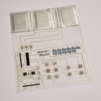
In 2010, the groundwork for PST Sensors was put in place. Harting and Britton negotiated the formation of the company and the assignment of the IP from UCT to PST once the shareholder's agreement was in place; as of 2011, the university is a minority shareholder and the South African government only receives a small royalty for its investment. The sensor technology was independently validated by Soligie, which has printed demonstration thermistors using PST inks. By Nov. 5, 2010, PST Sensors was formally registered as a limited company in South Africa.
Developing printed silicon was a huge challenge, and Britton said that stubbornness played a key role in seeing the challenge through.
“Apart from sheer bloody mindedness and a refusal to give up, the main factor is a combination of basic understanding of the materials, an appreciation of the requirements of the end-use applications and the imagination to see what is possible given the properties of the material,” Britton said. “For the printed silicon, this starts with the surface properties of our nanoparticles, which are electrically conducting and stable for years under ambient conditions and in the inks. The next is understanding the mechanisms of charge transport between individual particles and between clusters of particles, and then understanding the structure of the printed layer depending on all the processes used.”
Temperature sensors have proved to be a strong initial market for PST.
“Although we have a complete printed silicon electronics technology, the most important area for us in the near future is going to be sensors, specifically temperature sensors,” Britton said. “After time, temperature is the most measured quantity in applications in all sectors: health and leisure; automotive and aerospace; transport and logistics; food and consumer goods; white goods and consumer electronics; marketing and advertising.
“Conventional temperature sensors are widely used in all of these sectors, but often have distinct disadvantages resulting from their size, shape and packaging, as well as production cost,” Britton added. “Temperature mapping or averaging over large areas is simply not a practical proposition with a conventionally packaged (bead-type) thermistor or RTD, not the least because of poor thermal contact. Infrared thermography overcomes some of these disadvantages, but is imprecise and cannot ‘see’ inside an outer container.”
Since forming the company, PST Sensors has had a lot of interest, especially within the printed electronic sector from partners who have complementary technologies either on the market or at an advanced stage of development. Britton added that an announcement is expected shortly regarding joint development of particular applications with a major player in the field.
“There has also, obviously, been interest from materials suppliers in both directions (access to our materials and supply of complementary materials),” he added. “Other interest has come from independent product developers, system and product integrators, and some end-use customers who are still basically flagging the technology.”
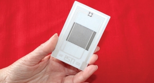
Britton said that PST is concentrating on developing its sensor technology, the latest being the thermal imaging mat, which is an array of individual sensors, with an eye on designing fully flexible sensors.
“The first version we showed at Printed Electronics USA consisted of 23 individually addressed sensors, which limits the number of elements which can be used,” Britton said. “In April, we intend to demonstrate a much higher resolution X-Y addressable array. The current generation of sensors are only conformable, not flexible. We have design prototypes of fully flexible sensors which will also be released next year.
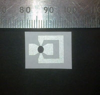
“Additionally, we are working on other sensor applications of printed silicon, including force and strain sensors, optical sensors (building on our early PV successes) and capacitive sensing (which we also demonstrated in 2009),” Britton added. “We are also collaborating with other partners on finding alternate materials, specifically to replace expensive materials like silver, but also to replace the harmful solvent-based systems used in existing commercial inks. An example of this was the tiger thermometer, which we produced in collaboration with NovaCentrix. We are also incorporating other passive elements into the printed circuitry, supplying a sensor system suited to the application, rather than a simple thermistor. In this respect we are also working with our partners and customers on product and system integration.”
Britton said that through close collaboration with the UCT NanoSciences Innovation Centre, PST Sensors continues to develop other aspects of the printed silicon platform, including not only the basic materials science, but also novel transistor architectures which play to the strengths of printed silicon, rather than trying to copy thin-film silicon or organic TFTs.
“This copycat approach was also ultimately what limited the technological progress with the printed silicon solar cells,” Britton added. “Recognizing that we are dealing with a different material with different properties to either crystalline or amorphous silicon, we are continuing the solar cell development (with more of an emphasis on research and education), through the NanoSciences Innovation Centre as part of a larger US/African network, Nano Power Africa, which has seed funding from USAID.”
Ultimately, Britton sees excellent opportunities for printed electronics, provided that the focus always remains on the customer.
“As long as we avoid the temptation to go head to head with established technologies, which are dominated by big players and cartels who have put in a lot of capital investment over many years, and avoid component replacement-type activities, the outlook is definitely good,” Britton concluded. “In specific areas, there are huge untapped accessible markets where conventional electronics, or non-electronic solutions, can't deliver or perform poorly. One area is sensing, another is energy harvesting (including PV), and a third is really large area (billboard size) electronics.
“But, we do have to get away from being simply component manufacturers or materials suppliers - what the end user requires is a ‘system.’ He or she doesn't care if it is printed or if it is based on the latest nanotechnology,” Britton added. “This means that different players in the sector have to work together to identify and deliver what the customer needs - so we have to work with the customers as well.”
PST Sensors is poised to make a major breakthrough in this field. Led by directors Margit Harting and David Britton, who have been working on this technology as professors at the University of Cape Town (UCT), PST Sensors has developed and proven its technology to print silicon semiconductors at room temperature on any material, including paper, using conventional printing methods.
|
|
Britton said that he and Harting have been working on the idea for more than a decade at the University of Cape Town.
“At the end of the 1990s, Margit and I were very much pure academics working on structural characterization hydrogenated amorphous silicon, grown by hot-wire CVD, and ultimately intended for PV applications,” Britton said. “This was a collaboration with Dirk Knoesen of our sister university, the University of the Western Cape, who was also collaborating with Werner van der Weg and Ruud Schropp at the University of Utrecht. We've both always been innovative in our science, and had some interesting breakthroughs like the first X-ray measurement of stress in an amorphous solid, which we could have taken further if we'd kept in our comfortable little box.
“Instead, we started getting involved in other aspects of thin film silicon technology, setting up our own optical and electronic characterization, and looking at applied aspects,” Britton added. “Most importantly, everyone was looking for a cheap flexible substrate, so in 2002, using Dirk's CVD equipment, we produced simple a-Si:H junction FETs on normal paper, followed by a very poor solar module.”
Britton and Harting found they could print their semiconductors, which opened up all sorts of possibilities.
“Apart from the silicon, all the other layers were printed using commercial inks,” Britton said. “Because we were printing everything else, and because there was a lot of hype about nano (especially in South Africa, where I was involved in drafting the National Nanotechnology Strategy Document), and because the best HW-CVD silicon was nanostructured, Margit came up with the idea of printing silicon nanoparticles. In 2003, we hand-printed J-FETS, using a rubber stamp cut from a pencil eraser, and silicon grinding powder in a binder made from a styrofoam cup dissolved in chloroform. It worked (badly!), and we filed the first patent.”
Harting and Britton saw the commercial possibilities of their technology, and began looking for backers and projects to commercialize. They chose photovoltaics (PV) as the initial target for their technology.
“Having made the decision not to go the normal academic route, we now started looking for funding to develop the technology, while continuing work using our limited research funds,” Britton recalled. “During this time we sorted out and filed patents on the basic materials aspects, including producing silicon nanoparticles by milling bulk silicon, and more useful ink bases. After a slow start, in 2005 we had agreement in principle from the South African Department of Science and Technology, through its business unit The Innovation Fund, to fund a three-year development project for ZAR 12.4 million (approximately $1.5M). We had to find a low hanging fruit so that at the end of the project we would have a prototype product and a realistic commercialization strategy. We chose low power portable PV, and the project started in July 2006.”
PV did not prove to be ideal, and Britton and Harting went back to the drawing board.
“Despite early successes with the PV, by the end of 2008 it was obvious to us that we had hit a ceiling with the technology, and it would need further research and development,” Britton said. “Also, the market was not ready for low power, portable, flexible PV. Progress in organic PV had been slower than we expected, and the first products were only just being introduced.”
To add to their initial difficulties, The Innovation Fund was being restructured and had to show return on investment, ultimately merging with several other agencies to form the Technology Innovation Agency.
“Our ‘commercialization strategy’ now had to be a full business plan,” Britton said. “We were able to extend the project by six months with no extra funding, and went back to the drawing board, around about the same time as the global recession hit VC funding. The first rewrite was for a technology development company for the printed silicon technology, which was seen as speculative and very high risk.”
With printed silicon, Britton and Harting found themselves trying to determine who they were competing against, what benefits their technology would offer and where their technology would fit in the market.
“PV wasn't market ready, and transistor logic would also need further development and had serious competition from thin-film Si and microelectronics,” Britton said. “Fully passive electronics would just make us one of thousands of thick-film companies, and supplying inks and pigments alone would put us at the bottom of the food chain.
|
|
In 2010, the groundwork for PST Sensors was put in place. Harting and Britton negotiated the formation of the company and the assignment of the IP from UCT to PST once the shareholder's agreement was in place; as of 2011, the university is a minority shareholder and the South African government only receives a small royalty for its investment. The sensor technology was independently validated by Soligie, which has printed demonstration thermistors using PST inks. By Nov. 5, 2010, PST Sensors was formally registered as a limited company in South Africa.
Developing printed silicon was a huge challenge, and Britton said that stubbornness played a key role in seeing the challenge through.
“Apart from sheer bloody mindedness and a refusal to give up, the main factor is a combination of basic understanding of the materials, an appreciation of the requirements of the end-use applications and the imagination to see what is possible given the properties of the material,” Britton said. “For the printed silicon, this starts with the surface properties of our nanoparticles, which are electrically conducting and stable for years under ambient conditions and in the inks. The next is understanding the mechanisms of charge transport between individual particles and between clusters of particles, and then understanding the structure of the printed layer depending on all the processes used.”
Temperature sensors have proved to be a strong initial market for PST.
“Although we have a complete printed silicon electronics technology, the most important area for us in the near future is going to be sensors, specifically temperature sensors,” Britton said. “After time, temperature is the most measured quantity in applications in all sectors: health and leisure; automotive and aerospace; transport and logistics; food and consumer goods; white goods and consumer electronics; marketing and advertising.
“Conventional temperature sensors are widely used in all of these sectors, but often have distinct disadvantages resulting from their size, shape and packaging, as well as production cost,” Britton added. “Temperature mapping or averaging over large areas is simply not a practical proposition with a conventionally packaged (bead-type) thermistor or RTD, not the least because of poor thermal contact. Infrared thermography overcomes some of these disadvantages, but is imprecise and cannot ‘see’ inside an outer container.”
Since forming the company, PST Sensors has had a lot of interest, especially within the printed electronic sector from partners who have complementary technologies either on the market or at an advanced stage of development. Britton added that an announcement is expected shortly regarding joint development of particular applications with a major player in the field.
“There has also, obviously, been interest from materials suppliers in both directions (access to our materials and supply of complementary materials),” he added. “Other interest has come from independent product developers, system and product integrators, and some end-use customers who are still basically flagging the technology.”
Britton said that PST is concentrating on developing its sensor technology, the latest being the thermal imaging mat, which is an array of individual sensors, with an eye on designing fully flexible sensors.
“The first version we showed at Printed Electronics USA consisted of 23 individually addressed sensors, which limits the number of elements which can be used,” Britton said. “In April, we intend to demonstrate a much higher resolution X-Y addressable array. The current generation of sensors are only conformable, not flexible. We have design prototypes of fully flexible sensors which will also be released next year.
“Additionally, we are working on other sensor applications of printed silicon, including force and strain sensors, optical sensors (building on our early PV successes) and capacitive sensing (which we also demonstrated in 2009),” Britton added. “We are also collaborating with other partners on finding alternate materials, specifically to replace expensive materials like silver, but also to replace the harmful solvent-based systems used in existing commercial inks. An example of this was the tiger thermometer, which we produced in collaboration with NovaCentrix. We are also incorporating other passive elements into the printed circuitry, supplying a sensor system suited to the application, rather than a simple thermistor. In this respect we are also working with our partners and customers on product and system integration.”
Britton said that through close collaboration with the UCT NanoSciences Innovation Centre, PST Sensors continues to develop other aspects of the printed silicon platform, including not only the basic materials science, but also novel transistor architectures which play to the strengths of printed silicon, rather than trying to copy thin-film silicon or organic TFTs.
“This copycat approach was also ultimately what limited the technological progress with the printed silicon solar cells,” Britton added. “Recognizing that we are dealing with a different material with different properties to either crystalline or amorphous silicon, we are continuing the solar cell development (with more of an emphasis on research and education), through the NanoSciences Innovation Centre as part of a larger US/African network, Nano Power Africa, which has seed funding from USAID.”
Ultimately, Britton sees excellent opportunities for printed electronics, provided that the focus always remains on the customer.
“As long as we avoid the temptation to go head to head with established technologies, which are dominated by big players and cartels who have put in a lot of capital investment over many years, and avoid component replacement-type activities, the outlook is definitely good,” Britton concluded. “In specific areas, there are huge untapped accessible markets where conventional electronics, or non-electronic solutions, can't deliver or perform poorly. One area is sensing, another is energy harvesting (including PV), and a third is really large area (billboard size) electronics.
“But, we do have to get away from being simply component manufacturers or materials suppliers - what the end user requires is a ‘system.’ He or she doesn't care if it is printed or if it is based on the latest nanotechnology,” Britton added. “This means that different players in the sector have to work together to identify and deliver what the customer needs - so we have to work with the customers as well.”