David Savastano, Editor04.17.13
With speakers from Microsoft Research, Abbott Pharmaceuticals, Boeing, Philips and other industry leaders, Printed Electronics Europe 2013 opened its doors on April 17 for its two-day conference at the International Congress Centrum (ICC) in Berlin, Germany.
The focus of the day’s talks was on opportunities, with speakers from major corporations and entrepreneurial start-ups alike discussing the work they are doing in the PE field.
Raghu Das, CEO of IDTechEx, the conference’s organizer, opened the conference with his talk, "Printed Electronics: Show Me the Money." Das noted that printed electronics is an umbrella term that covers printed, organic and flexible electronics.
“Printed electronics is a disruptive technology,” Das said. “Some companies are trying to replace whole existing devices, such as OLED displays and lighting. These are high risk, high reward opportunities. Other companies are looking to improve on existing layers or components, such as by reducing cost or improving performance. Others are looking to create new markets, such as eReaders.”
Das noted that there are three billon-dollar markets so far: OLED, which is not printed yet, eReaders and conductive inks, most of which are used in photovoltaics. He said he is seeing a shift toward companies moving away from the idea of replacing whole devices to taking on smaller projects.
“Companies are transitioning to shorter-term, easier projects,” Das added.
Dr. Alex Butler, senior research hardware engineer, Microsoft Research, then covered "The Future of Touch/Enabling Technologies."
“Touch is ubiquitous now,” Dr. Butler said. “Touch is deployable everywhere. Now we want to do this with every display we see. History shows that new hardware leads to new software and new experiences. Unbreakable, flexible and curved displays are an exciting and under-exploited future potential.”
Dr. Sophie Laurenson, project lead for Abbott Diagnostics, analyzed "Printed Electronics for the Diagnostics Industry." The in vitro diagnostics (IVD) market is a $6 billion field, with $3 billion used in core laboratory testing. Dr. Laurenson said that printed sensors already detect glucose, and there are more opportunities ahead.
“Many components in current and future diagnostic products could be produced using processes designed for the printed electronics industry,” Dr. Laurenson noted.
Jeff Duce, design engineer, Boeing Research & Technology, gave his presentation on "Applications, Needs and Requirements for Printed Electronics in Aerospace." Duce said that weight reduction can save on fuel costs, which is of major interest to the airlines, and PE can find opportunities in areas such as lighting, wiring and displays.
“A 1% weight reduction in airplanes could equate to billions o dollars saved in operating cost,” Duce said. “We see printed electronics as an enabler. Boeing is hungry for new developments in printed electronics.”
Koen van Os, senior scientist intelligent at Philips Research, offered his insights into "Intelligent Textiles: Bridging the Gap from Technology Development to Product Manufacturing."
Van Os noted that conductive textiles have actually been around since the days of gold embroidered clothing, and companies have been putting in wires into clothing recently. He spoke about the BlueTouch system that Philips is developing for the healthcare field.
Van Os said that there are three entry points for intelligent textiles. The first is hybrid processing, using wires. The second is heterogenous, which offers stretchability. The third is homogenous, in which the entire material itself is conductive.
“We can make inexpensive, robust, sustainable and wearable electronics,” Van Os concluded.
Eric Penot, digital media director, JCDecaux, discussed outdoor digital advertising in his talk on "Digital Of-Home Industry Needs."
Penot noted that JCDecaux has more than 12,000 digital screens and billboards globally, and is looking for ways to improve its systems. “We have a lot of needs,” Penot said.
Dr. Juha Maijala, manager, intelligent solutions for Stora Enso, offered his insights into "Packages with Additional Intelligent Functionality," with an emphasis on intelligent healthcare packaging. Stora Enso has developed a number of solutions in this area.
“Cost efficiency is crucial,” Dr. Maijala said. “Its niche is high value special products.”
Dr. Simon Leigh, research fellow, University of Warwick, concluded the keynote talks with "3D Printed Electronics." Dr. Leigh said that presently, 3D printing is primarily done by micro stereolithography and fluid deposition, and added that he sees opportunities for printed electronics in the future.
After the keynote section, the conference broke into four concurrent sessions, with a wide variety of interesting companies and researchers presenting their latest developments.
Track 3, TCF LIVE!, looked at transparent conductive films, and featured some leading PE innovators discussing Sensor Technology Developments. Laurent Jamet, ISORG’s co-founder and director business development, led off with "When Printed Electronics Meet Design and Usages for Highly Innovative Functionalities."
ISORG’s organic photosensors transform plastic, paper and glass into smart and interactive surfaces.
“Our fully integrated organic photosensors are a fully printed process that is air and temperature ambient and is produced sheet to sheet,” James said. “These are thin, light robust and flexible sensors. We create a large area optical sensor with no need for optical elements, and have also developed gesture recognition at a short distance.”
James noted that ISORG is reaching commercialization now.
“Our pilot production line began in 2012,” James said. “We are transferring the technology to the market now, with mass production starting next year. Target applications include medical and health, such as sensors for digital x-ray imaging, pharmacy and diagnostics; industrial; and consumer markets, which includes smart phones and tablets, appliances, image sensors, smart textiles and smart packaging.”
Peratech Ltd. CTO David Lussey discussed "Quantum Tunnelling Composites (QTC) in Switches, Sensors, Controls and Touch Screens." Lussey said that QTCs are a new breed of electrical composites, and are a combination of polymer and conductive filler.
“QTCs respond to a variety of stimuli,” Lussey said. “It is extremely sensitive to small inputs of mechanical energy or electrical charges - pressure including touch, sound and vibration, voltage, temperature, VOCs and electromagnetic radiation.
“Shaped conductive and semi-conductive particulates produce field emission tunnelling conduction with QTCs,” Lussey added. “It only conducts where there is pressure, which means that I can make touch screens that no one else can. They can be made as a solid, powder, coating or ink.”
QTC has already appeared on the markets, such for jackets, but the main use is for telephone touch screens. “There are thousands of ways QTCs can be used,” Lussey concluded.
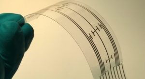
Linköping University associate professor Dr. Isak Engquist discussed "Printed Wireless Humidity Sensors for Moisture Detection in Buildings."
“For us, the challenge was moisture damage in buildings, and 750,000 buildings are affected in Sweden alone,” Dr. Engquist said. “The damage is often invisible at first, and testing is difficult as homeowners don’t want to put holes in walls, and wireless sensors are expensive. “
To solve this problem, Linköping University developed a humidity sensor label that is fully printed on a flexible substrate with a roll-to-roll patterned antenna.
“We came up with printed flexible sensor labels with no battery that are low cost, so you could use many sensors in a building, and it can be read by portable sensors,” Dr. Engquist said.
Prof. Margit Harting, Department of Physics at Cape Town University and PST Sensors, offered her thoughts on "Printed Silicon in Electronics."
Harting noted that PST Sensors is a 2010 spin-out from Cape Town University, with its first Printed Silicon inks used on thermistors launched in April 2011. These Printed Silicon inks can be used for transistors/logic, solar cells and sensors/arrays.
“Silicon is an amazing materials,” Harding said. “It is abundant, low cost and does not degrade. It is also temperature sensitive.”
PST’s thermistors are temperature sensitive resistors printed with silicon nano-particle inks.
“Thermistors contribute to more than 25% of the sensor market,” Harding said. “Temperature is the second-most often measured physical quantity behind time. It is important for a wide range of applications, such as packaging, healthcare environmental comfort, structural health of airplanes and process control. It is a growth market.”
OLEDs LIVE! was the focus of Track 2. Dr. Ton van Mol, program manager, TNO Holst Centre, analyzed "Flexible OLED Lighting."
“People will eventually go to roll-to-roll,” Dr. van Mol said. “The technology change is pretty significant. We think that in the meantime, people will go to a foil or barrier film substrate.Holst Center is developing key technologies to help transition from glass-based to flexible substrates, including bonding/debonding technology, a three-layer thin film barrier technology and a low temperature transparent conductor process.
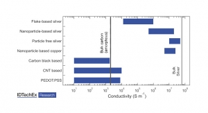
“We are focusing on copper plating and silver printing, replacing ITO with high conductive PEDOT:PSS,” Dr. van Nol added. “We are screen printing and using in-line photonic sintering. Silver is expensive, so we are working on copper nanoparticle inks.”
New OLED Material Developments was the final topic of OLEDs LIVE! Dr. Silvia Janietz, head of polymers and electronics, Fraunhofer IAP, discussed "Integration of OLEDs in Textiles.”
“Integrating OLEDs into textiles is a promising field,” Dr. Janietz said, noting that wellness and care, protection, information, fashion and sports are potential areas of interest. “Encapsulated glass OLEDs are stiff and have comparatively big dimensions.”
One approach is to use spacer warp knitting to integrate the glass OLEDs. A flexible OLED foil strip was also applied, and hot lamination had no influence on performance.
“Integration of planar OLEDs in special textiles with spacer thin knitting was realized,” Dr. Janietz said.
Cynora GmbH CEO Dr. Tobias Grab closed OLEDs LIVE! with his talk on "Optoelectronic Solutions for OLEDs." Cynora focuses on copper-based emitter compounds and customized solutions.
“We want to develop individual optoelectronic solutions for our customers,” Dr. Grab said.
The focus of the day’s talks was on opportunities, with speakers from major corporations and entrepreneurial start-ups alike discussing the work they are doing in the PE field.
Raghu Das, CEO of IDTechEx, the conference’s organizer, opened the conference with his talk, "Printed Electronics: Show Me the Money." Das noted that printed electronics is an umbrella term that covers printed, organic and flexible electronics.
“Printed electronics is a disruptive technology,” Das said. “Some companies are trying to replace whole existing devices, such as OLED displays and lighting. These are high risk, high reward opportunities. Other companies are looking to improve on existing layers or components, such as by reducing cost or improving performance. Others are looking to create new markets, such as eReaders.”
Das noted that there are three billon-dollar markets so far: OLED, which is not printed yet, eReaders and conductive inks, most of which are used in photovoltaics. He said he is seeing a shift toward companies moving away from the idea of replacing whole devices to taking on smaller projects.
“Companies are transitioning to shorter-term, easier projects,” Das added.
Dr. Alex Butler, senior research hardware engineer, Microsoft Research, then covered "The Future of Touch/Enabling Technologies."
“Touch is ubiquitous now,” Dr. Butler said. “Touch is deployable everywhere. Now we want to do this with every display we see. History shows that new hardware leads to new software and new experiences. Unbreakable, flexible and curved displays are an exciting and under-exploited future potential.”
Dr. Sophie Laurenson, project lead for Abbott Diagnostics, analyzed "Printed Electronics for the Diagnostics Industry." The in vitro diagnostics (IVD) market is a $6 billion field, with $3 billion used in core laboratory testing. Dr. Laurenson said that printed sensors already detect glucose, and there are more opportunities ahead.
“Many components in current and future diagnostic products could be produced using processes designed for the printed electronics industry,” Dr. Laurenson noted.
Jeff Duce, design engineer, Boeing Research & Technology, gave his presentation on "Applications, Needs and Requirements for Printed Electronics in Aerospace." Duce said that weight reduction can save on fuel costs, which is of major interest to the airlines, and PE can find opportunities in areas such as lighting, wiring and displays.
“A 1% weight reduction in airplanes could equate to billions o dollars saved in operating cost,” Duce said. “We see printed electronics as an enabler. Boeing is hungry for new developments in printed electronics.”
Koen van Os, senior scientist intelligent at Philips Research, offered his insights into "Intelligent Textiles: Bridging the Gap from Technology Development to Product Manufacturing."
Van Os noted that conductive textiles have actually been around since the days of gold embroidered clothing, and companies have been putting in wires into clothing recently. He spoke about the BlueTouch system that Philips is developing for the healthcare field.
Van Os said that there are three entry points for intelligent textiles. The first is hybrid processing, using wires. The second is heterogenous, which offers stretchability. The third is homogenous, in which the entire material itself is conductive.
“We can make inexpensive, robust, sustainable and wearable electronics,” Van Os concluded.
Eric Penot, digital media director, JCDecaux, discussed outdoor digital advertising in his talk on "Digital Of-Home Industry Needs."
Penot noted that JCDecaux has more than 12,000 digital screens and billboards globally, and is looking for ways to improve its systems. “We have a lot of needs,” Penot said.
Dr. Juha Maijala, manager, intelligent solutions for Stora Enso, offered his insights into "Packages with Additional Intelligent Functionality," with an emphasis on intelligent healthcare packaging. Stora Enso has developed a number of solutions in this area.
“Cost efficiency is crucial,” Dr. Maijala said. “Its niche is high value special products.”
Dr. Simon Leigh, research fellow, University of Warwick, concluded the keynote talks with "3D Printed Electronics." Dr. Leigh said that presently, 3D printing is primarily done by micro stereolithography and fluid deposition, and added that he sees opportunities for printed electronics in the future.
After the keynote section, the conference broke into four concurrent sessions, with a wide variety of interesting companies and researchers presenting their latest developments.
Track 3, TCF LIVE!, looked at transparent conductive films, and featured some leading PE innovators discussing Sensor Technology Developments. Laurent Jamet, ISORG’s co-founder and director business development, led off with "When Printed Electronics Meet Design and Usages for Highly Innovative Functionalities."
ISORG’s organic photosensors transform plastic, paper and glass into smart and interactive surfaces.
“Our fully integrated organic photosensors are a fully printed process that is air and temperature ambient and is produced sheet to sheet,” James said. “These are thin, light robust and flexible sensors. We create a large area optical sensor with no need for optical elements, and have also developed gesture recognition at a short distance.”
James noted that ISORG is reaching commercialization now.
“Our pilot production line began in 2012,” James said. “We are transferring the technology to the market now, with mass production starting next year. Target applications include medical and health, such as sensors for digital x-ray imaging, pharmacy and diagnostics; industrial; and consumer markets, which includes smart phones and tablets, appliances, image sensors, smart textiles and smart packaging.”
Peratech Ltd. CTO David Lussey discussed "Quantum Tunnelling Composites (QTC) in Switches, Sensors, Controls and Touch Screens." Lussey said that QTCs are a new breed of electrical composites, and are a combination of polymer and conductive filler.
“QTCs respond to a variety of stimuli,” Lussey said. “It is extremely sensitive to small inputs of mechanical energy or electrical charges - pressure including touch, sound and vibration, voltage, temperature, VOCs and electromagnetic radiation.
“Shaped conductive and semi-conductive particulates produce field emission tunnelling conduction with QTCs,” Lussey added. “It only conducts where there is pressure, which means that I can make touch screens that no one else can. They can be made as a solid, powder, coating or ink.”
QTC has already appeared on the markets, such for jackets, but the main use is for telephone touch screens. “There are thousands of ways QTCs can be used,” Lussey concluded.
Linköping University associate professor Dr. Isak Engquist discussed "Printed Wireless Humidity Sensors for Moisture Detection in Buildings."
“For us, the challenge was moisture damage in buildings, and 750,000 buildings are affected in Sweden alone,” Dr. Engquist said. “The damage is often invisible at first, and testing is difficult as homeowners don’t want to put holes in walls, and wireless sensors are expensive. “
To solve this problem, Linköping University developed a humidity sensor label that is fully printed on a flexible substrate with a roll-to-roll patterned antenna.
“We came up with printed flexible sensor labels with no battery that are low cost, so you could use many sensors in a building, and it can be read by portable sensors,” Dr. Engquist said.
Prof. Margit Harting, Department of Physics at Cape Town University and PST Sensors, offered her thoughts on "Printed Silicon in Electronics."
Harting noted that PST Sensors is a 2010 spin-out from Cape Town University, with its first Printed Silicon inks used on thermistors launched in April 2011. These Printed Silicon inks can be used for transistors/logic, solar cells and sensors/arrays.
“Silicon is an amazing materials,” Harding said. “It is abundant, low cost and does not degrade. It is also temperature sensitive.”
PST’s thermistors are temperature sensitive resistors printed with silicon nano-particle inks.
“Thermistors contribute to more than 25% of the sensor market,” Harding said. “Temperature is the second-most often measured physical quantity behind time. It is important for a wide range of applications, such as packaging, healthcare environmental comfort, structural health of airplanes and process control. It is a growth market.”
OLEDs LIVE! was the focus of Track 2. Dr. Ton van Mol, program manager, TNO Holst Centre, analyzed "Flexible OLED Lighting."
“People will eventually go to roll-to-roll,” Dr. van Mol said. “The technology change is pretty significant. We think that in the meantime, people will go to a foil or barrier film substrate.Holst Center is developing key technologies to help transition from glass-based to flexible substrates, including bonding/debonding technology, a three-layer thin film barrier technology and a low temperature transparent conductor process.
“We are focusing on copper plating and silver printing, replacing ITO with high conductive PEDOT:PSS,” Dr. van Nol added. “We are screen printing and using in-line photonic sintering. Silver is expensive, so we are working on copper nanoparticle inks.”
New OLED Material Developments was the final topic of OLEDs LIVE! Dr. Silvia Janietz, head of polymers and electronics, Fraunhofer IAP, discussed "Integration of OLEDs in Textiles.”
“Integrating OLEDs into textiles is a promising field,” Dr. Janietz said, noting that wellness and care, protection, information, fashion and sports are potential areas of interest. “Encapsulated glass OLEDs are stiff and have comparatively big dimensions.”
One approach is to use spacer warp knitting to integrate the glass OLEDs. A flexible OLED foil strip was also applied, and hot lamination had no influence on performance.
“Integration of planar OLEDs in special textiles with spacer thin knitting was realized,” Dr. Janietz said.
Cynora GmbH CEO Dr. Tobias Grab closed OLEDs LIVE! with his talk on "Optoelectronic Solutions for OLEDs." Cynora focuses on copper-based emitter compounds and customized solutions.
“We want to develop individual optoelectronic solutions for our customers,” Dr. Grab said.