07.03.15
Imec and its partners successfully completed a three-year program (2012-2015) to leverage a variety of silicon photonics technologies by making them accessible for industry and academia worldwide. Within the ESSenTIAL program funded by the European Commission, imec worked closely with CEA-LETI (France), Tyndall Institute (Ireland), VTT (Finland), IHP (Germany), TNO (The Netherlands) and CMC (Canada) to develop advanced multi-project-wafer services as well as packaging services for silicon photonics.
The services were made accessible to industrial players – both small- and medium-sized companies – enabling them to test silicon photonics technology.
Silicon photonics is a key enabling technology for a wide range of markets, from optical interconnect networks in data centers to disposable biosensor chips for immunoassays. Silicon photonics builds on the technology portfolio and economy of scale of CMOS fabs to manufacture sophisticated photonic integrated circuits with a combination of passive devices – in particular wavelength and polarization selective devices – and active devices such as optical modulators and detectors.
The ESSenTIAL program has extensively expanded the services of ePIXfab, an alliance of European entities set up in 2006 to support the emergence of a fabless silicon photonics ecosystem. ePIXfab has provided affordable Multi-Project Wafer (MPW) services to fabless R&D teams worldwide developing photonic circuits. European users received some benefits based on EU funding, but the ePIXfab services were provided globally.
“ePIXfab was founded to provide the silicon photonics research community an access path to advanced CMOS technology with the goal of sharing cost and expertise. ePIXfab has helped to accelerate the field of silicon photonics and to let it move from a research field to a field of critical industrial importance,” says Ghent University professor Roel Baets, one of the founders of ePIXfab and research team leader associated with imec.
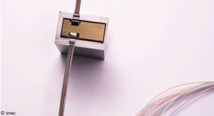
In total, more than 200 silicon photonics circuit designs were prototyped at imec, LETI, IHP or VTT, including close to 50 designs from companies. Another major achievement of the project was the creation of silicon photonics packaging services at Tyndall Institute.
”Packaging is often seen as the Achilles heel of photonic component technology. Tyndall Institute has developed a family of solutions, encompassing optical, electrical and RF packaging. These standardized packaging approaches for silicon photonic chips are available to industry through the ePIXfab-alliance,” said Peter O’Brien, head of the Photonics Packaging Group at Tyndall.
During ESSenTIAL the MPW operation for silicon photonics has been integrated into Europractice IC service, marking a milestone for the further growth of Europe’s silicon photonics.
ePIXfab is open to new European members. For more information, contact Prof. Roel Baets ([email protected]).
The services were made accessible to industrial players – both small- and medium-sized companies – enabling them to test silicon photonics technology.
Silicon photonics is a key enabling technology for a wide range of markets, from optical interconnect networks in data centers to disposable biosensor chips for immunoassays. Silicon photonics builds on the technology portfolio and economy of scale of CMOS fabs to manufacture sophisticated photonic integrated circuits with a combination of passive devices – in particular wavelength and polarization selective devices – and active devices such as optical modulators and detectors.
The ESSenTIAL program has extensively expanded the services of ePIXfab, an alliance of European entities set up in 2006 to support the emergence of a fabless silicon photonics ecosystem. ePIXfab has provided affordable Multi-Project Wafer (MPW) services to fabless R&D teams worldwide developing photonic circuits. European users received some benefits based on EU funding, but the ePIXfab services were provided globally.
“ePIXfab was founded to provide the silicon photonics research community an access path to advanced CMOS technology with the goal of sharing cost and expertise. ePIXfab has helped to accelerate the field of silicon photonics and to let it move from a research field to a field of critical industrial importance,” says Ghent University professor Roel Baets, one of the founders of ePIXfab and research team leader associated with imec.
In total, more than 200 silicon photonics circuit designs were prototyped at imec, LETI, IHP or VTT, including close to 50 designs from companies. Another major achievement of the project was the creation of silicon photonics packaging services at Tyndall Institute.
”Packaging is often seen as the Achilles heel of photonic component technology. Tyndall Institute has developed a family of solutions, encompassing optical, electrical and RF packaging. These standardized packaging approaches for silicon photonic chips are available to industry through the ePIXfab-alliance,” said Peter O’Brien, head of the Photonics Packaging Group at Tyndall.
During ESSenTIAL the MPW operation for silicon photonics has been integrated into Europractice IC service, marking a milestone for the further growth of Europe’s silicon photonics.
ePIXfab is open to new European members. For more information, contact Prof. Roel Baets ([email protected]).