03.13.18
A new method to produce large, monolayer single-crystal-like graphene films more than a foot long relies on harnessing a “survival of the fittest” competition among crystals. The technique, developed by a team led by the Department of Energy’s Oak Ridge National Laboratory (ORNL), may open new opportunities for growing the high-quality two-dimensional materials necessary for long-awaited practical applications.
Making thin layers of graphene and other 2D materials on a scale required for research purposes is common, but they must be manufactured on a much larger scale to be useful.
Graphene is touted for its potential of unprecedented strength and high electrical conductivity and can be made through well-known approaches: separating flakes of graphite – the silvery soft material found in pencils – into one-atom-thick layers, or growing it atom by atom on a catalyst from a gaseous precursor until ultrathin layers are formed.
The ORNL-led research team used the latter method – known as chemical vapor deposition, or CVD – but with a twist. In a study published in Nature Materials, they explained how localized control of the CVD process allows evolutionary, or self-selecting, growth under optimal conditions, yielding a large, single-crystal-like sheet of graphene.
“Large single crystals are more mechanically robust and may have higher conductivity,” ORNL lead coauthor Ivan Vlassiouk said. “This is because weaknesses arising from interconnections between individual domains in polycrystalline graphene are eliminated. Our method could be the key not only to improving large-scale production of single-crystal graphene but to other 2D materials as well, which is necessary for their large-scale applications.”
Much like traditional CVD approaches to produce graphene, the researchers sprayed a gaseous mixture of hydrocarbon precursor molecules onto a metallic, polycrystalline foil. However, they carefully controlled the local deposition of the hydrocarbon molecules, bringing them directly to the edge of the emerging graphene film. As the substrate moved underneath, the carbon atoms continuously assembled as a single crystal of graphene up to a foot in length.
“The unencumbered single-crystal-like graphene growth can go almost continuously, as a roll-to-roll and beyond the foot-long samples demonstrated here,” said Sergei Smirnov, co-author and New Mexico State University professor.
As the hydrocarbons touch down the hot catalyst foil, they form clusters of carbon atoms that grow over time into larger domains until coalescing to cover the whole substrate. The team previously found that at sufficiently high temperatures, the carbon atoms of graphene did not correlate, or mirror, the substrate’s atoms, allowing for nonepitaxial crystalline growth.
They found that to ensure optimal growth, it was necessary to create a “wind” that helps to eliminate the cluster formations. “It was imperative that we create an environment where the formation of new clusters ahead of the growth front was totally suppressed, and enlargement of just the growing edge of the large graphene crystal was not hindered,” Vlassiouk said. “Then, and only then, nothing stands in the way of the ‘fittest’ crystalline growth when the substrate is moving.”
The team’s theoreticians, led by co-author Rice University professor Boris Yakobson, provided a model explaining which crystal orientations possess the unique properties that make them fittest in the run for survival, and why the choice of a winner may depend on the substrate and the precursors.
“If graphene or any 2D material ever advances to industrial scale, this approach will be pivotal, similar to Czochralski’s method for silicon.” Yakobson said. “Manufacturers can rest assured that when a large, wafer-size raw layer is cut for any device fabrication, each resulting piece will be a quality monocrystal. This potentially huge, impactful role motivates us to explore theoretical principles to be as clear as possible.”
The team’s paper, “Evolutionary selection growth of two-dimensional materials on polycrystalline substrates,” included coauthors Ivan Vlassiouk, Yijing Stehle, Raymond R. Unocic, Arthur P. Baddorf, Ilia N. Ivanov, Nickolay V. Lavrik and Frederick List of Oak Ridge National Laboratory; Philip D. Rack of ORNL and University of Tennessee; Pushpa Raj Pudasini of UT; Nitant Gupta, Ksenia Bets and Boris I. Yakobson of Rice University; and Sergei Smirnov of New Mexico State University.
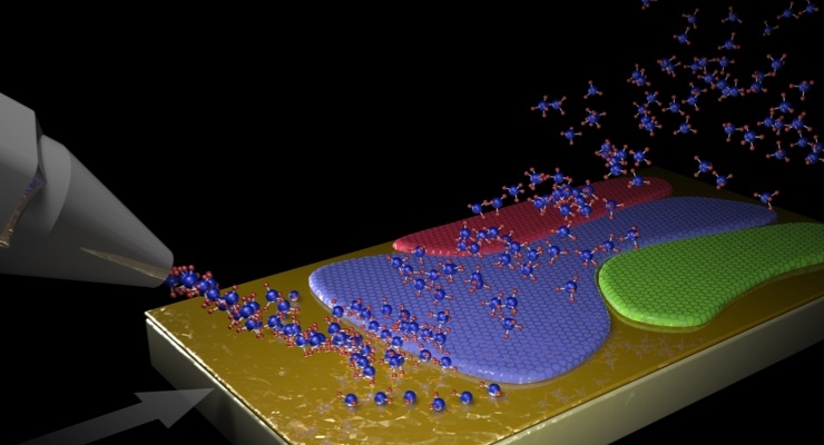
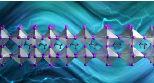
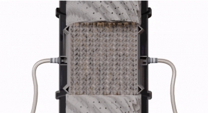
n a controlled environment, the fastest-growing orientation of graphene crystals overwhelms the others and gets “evolutionarily selected” into a single crystal, even on a polycrystalline substrate, without having to match the substrate’s orientation. An Oak Ridge National Laboratory-led team developed the novel method that produces large, monolayer single-crystal-like graphene films more than a foot long. Credit: Andy Sproles/Oak Ridge National Laboratory, US Dept. of Energy.
Making thin layers of graphene and other 2D materials on a scale required for research purposes is common, but they must be manufactured on a much larger scale to be useful.
Graphene is touted for its potential of unprecedented strength and high electrical conductivity and can be made through well-known approaches: separating flakes of graphite – the silvery soft material found in pencils – into one-atom-thick layers, or growing it atom by atom on a catalyst from a gaseous precursor until ultrathin layers are formed.
The ORNL-led research team used the latter method – known as chemical vapor deposition, or CVD – but with a twist. In a study published in Nature Materials, they explained how localized control of the CVD process allows evolutionary, or self-selecting, growth under optimal conditions, yielding a large, single-crystal-like sheet of graphene.
“Large single crystals are more mechanically robust and may have higher conductivity,” ORNL lead coauthor Ivan Vlassiouk said. “This is because weaknesses arising from interconnections between individual domains in polycrystalline graphene are eliminated. Our method could be the key not only to improving large-scale production of single-crystal graphene but to other 2D materials as well, which is necessary for their large-scale applications.”
Much like traditional CVD approaches to produce graphene, the researchers sprayed a gaseous mixture of hydrocarbon precursor molecules onto a metallic, polycrystalline foil. However, they carefully controlled the local deposition of the hydrocarbon molecules, bringing them directly to the edge of the emerging graphene film. As the substrate moved underneath, the carbon atoms continuously assembled as a single crystal of graphene up to a foot in length.
“The unencumbered single-crystal-like graphene growth can go almost continuously, as a roll-to-roll and beyond the foot-long samples demonstrated here,” said Sergei Smirnov, co-author and New Mexico State University professor.
As the hydrocarbons touch down the hot catalyst foil, they form clusters of carbon atoms that grow over time into larger domains until coalescing to cover the whole substrate. The team previously found that at sufficiently high temperatures, the carbon atoms of graphene did not correlate, or mirror, the substrate’s atoms, allowing for nonepitaxial crystalline growth.
They found that to ensure optimal growth, it was necessary to create a “wind” that helps to eliminate the cluster formations. “It was imperative that we create an environment where the formation of new clusters ahead of the growth front was totally suppressed, and enlargement of just the growing edge of the large graphene crystal was not hindered,” Vlassiouk said. “Then, and only then, nothing stands in the way of the ‘fittest’ crystalline growth when the substrate is moving.”
The team’s theoreticians, led by co-author Rice University professor Boris Yakobson, provided a model explaining which crystal orientations possess the unique properties that make them fittest in the run for survival, and why the choice of a winner may depend on the substrate and the precursors.
“If graphene or any 2D material ever advances to industrial scale, this approach will be pivotal, similar to Czochralski’s method for silicon.” Yakobson said. “Manufacturers can rest assured that when a large, wafer-size raw layer is cut for any device fabrication, each resulting piece will be a quality monocrystal. This potentially huge, impactful role motivates us to explore theoretical principles to be as clear as possible.”
The team’s paper, “Evolutionary selection growth of two-dimensional materials on polycrystalline substrates,” included coauthors Ivan Vlassiouk, Yijing Stehle, Raymond R. Unocic, Arthur P. Baddorf, Ilia N. Ivanov, Nickolay V. Lavrik and Frederick List of Oak Ridge National Laboratory; Philip D. Rack of ORNL and University of Tennessee; Pushpa Raj Pudasini of UT; Nitant Gupta, Ksenia Bets and Boris I. Yakobson of Rice University; and Sergei Smirnov of New Mexico State University.
n a controlled environment, the fastest-growing orientation of graphene crystals overwhelms the others and gets “evolutionarily selected” into a single crystal, even on a polycrystalline substrate, without having to match the substrate’s orientation. An Oak Ridge National Laboratory-led team developed the novel method that produces large, monolayer single-crystal-like graphene films more than a foot long. Credit: Andy Sproles/Oak Ridge National Laboratory, US Dept. of Energy.