• Login
    • Join
  • FOLLOW:
  • Subscribe Free
    • Magazine
    • eNewsletter
    Checkout
    • Magazine
    • News
    • Printed Electronics
    • Raw Materials
    • Equipment
    • Services
    • Suppliers Guide
    • Resources
    • More
  • Magazine
  • News
  • Printed Electronics
  • Raw Materials
  • Equipment
  • Services
  • Suppliers Guide
  • Resources
  • Current & Past Issues
    Features
    Editorials
    Digital Edition
    Subscribe Now
    Advertise Now
    eNewsletter Archive
    Our Team
    Editorial Guidelines
    Breaking News
    Experts Opinion
    Financial News
    Manufacturers News
    Mergers and Acquisitions
    Online Exclusives
    Personnel
    Product Releases
    Suppliers News
    Live From Shows
    Displays and Lighting
    Photovoltaics
    Printed Batteries
    Printed Circuit Boards/Membrane Switches/In Mold Electronics
    Flexible and Printed Electronics
    RFID and NFC
    Sensors and Wearables
    Smart Cards and Packaging
    Touch Screens
    Adhesives, Barriers and Encapsulants
    Chemicals, Metals and Powders
    Conductive Inks and Coatings
    Electronic Materials
    Film, Paper, Glass and Substrates
    Graphene, Perovskites and Carbon Nanotubes
    Nanomaterials
    Printed Electronic Components
    Research Reports
    Semiconductors and Quantum Dots
    Energy Curing Equipment
    Lab and Testing Equipment
    Manufacturing Equipment
    Printing Equipment
    3D Printing
    Contract Manufacturing Services
    Product Design and Testing
    Research and Consulting
    Research Institutions
    Research Reports
    Universities
    Equipment
    All Companies
    Materials
    Categories
    Converting
    Printed Electronics Systems
    Associations
    Research and Services
    Used Machinery
    Add New Company
    Industry Events
    Live from show events
    Podcasts
    Videos
    Blogs
    Slideshows
    Infographics
    Webinars
    Whitepapers
    Equipment and Services
    Glossary
    • Magazine
      • Current & Past Issues
      • Features
      • Editorial
      • Columns
      • Digital Edition
      • eNewsletter Archive
      • Editorial Guidelines
      • Subscribe Now
      • Advertise Now
    • Breaking News
    • Suppliers Guide
      • Suppliers Guide
      • Add Your Company
    • Printed Electronics
      • Photovoltaics
      • Printed Batteries
      • Printed Circuit Boards/Membrane Switches/In Mold Electronics
      • Flexible and Printed Electronics
      • RFID and NFC
      • Sensors and Wearables
      • Smart Cards and Packaging
      • Touch Screens
    • Raw Materials
      • Adhesives, Barriers and Encapsulants
      • Chemicals, Metals and Powders
      • Conductive Inks and Coatings
      • Electronic Materials
      • Film, Paper, Glass and Substrates
      • Graphene, Perovskites and Carbon Nanotubes
      • Nanomaterials
      • Semiconductors and Quantum Dots
    • Equipment
      • Energy Curing Equipment
      • Lab and Testing Equipment
      • Manufacturing Equipment
      • Printing Equipment
      • 3D Printing
    • Services
      • Contract Manufacturing Services
      • Product Design and Testing
      • Research and Consulting
      • Research Institutions
      • Research Reports
      • Universities
    • Online Exclusives
    • Slideshows
    • Blog
    • Videos
    • Podcasts
    • Infographics
    • Events
      • Industry Events
      • Live from show events
      • Webinars
    • About Us
      • About Us
      • Contact Us
      • Advertise With Us
      • Privacy Policy
      • Terms of Use
    Breaking News

    Imec Reports Direct Growth of 2D Materials on 300mm Wafers for First Time

    2D materials could provide the path towards extreme device-dimension scaling.

    Related CONTENT
    • Imec’s Ultrasound Sensor Technology Helps Determine Arterial Stiffness
    • Tandem Breakthrough by Solliance Partners
    • SEMI Appoints imec, Soitec Executives to Europe Advisory Board
    • imec: Decade of R&D Establishes Europe in Thin-film PV
    • Imec Demonstrates Ultra-sensitive, Small Optomechanical Ultrasound Sensor in Silicon Photonics
    12.04.18
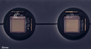
    This week, at the 2018 IEEE International Electron Devices Meeting (IEDM), imec presents a 300mm-wafer platform for MOSFET devices with 2D materials. 2D materials could provide the path towards extreme device-dimension scaling as they are atomically precise and suffer little from short channel effects. Other possible applications of 2D materials could come from using them as switches in the BEOL, which puts an upper limit on the allowed temperature budget in the integration flow.
     
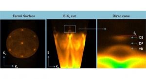
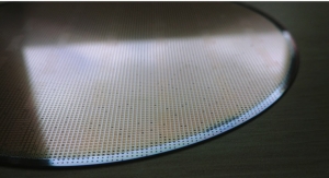
    The imec platform integrates as transistor channel WS2, a 2D material which holds promise for higher ON current compared to most other 2D materials and good chemical stability. Imec reports here for the first time the MOCVD growth of WS2 on 300mm wafers, a key process step for device fabrication. The benefits of the MOCVD growth come at the price of a high temperature while growing the material.
     
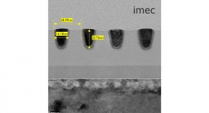
    To build a device integration flow which could be compatible with BEOL requirements, the transfer of the channel material from a growth substrate to a device wafer is crucial. Imec is the first to demonstrate a full 300mm monolayer 2D material transfer, which is challenging on its own because of the low adhesion of 2D materials to the device wafer and to the extreme thinness of the material transferred: 0.7nm.
     
    The transfer process was developed together with SUSS MicroTec and Brewer Science using temporary bonding and debonding technologies. WS2 wafers are temporarily bonded to glass carrier wafers using a specially formulated material (Brewer Science). Next, the WS2 monolayer is mechanically debonded from the growth wafer and bonded again in vacuum to the device wafer. The carrier wafer is removed using laser debonding. This debonding technique is a key enabler for the controlled transfer of 2D materials
     
    “Building the 300mm platform for MOSFET device study with 2D materials and developing the process step ecosystem speeds-up the technological adoption of these materials,” Iuliana Radu, Beyond CMOS program director at imec, said. “Several challenges are still to be resolved and are the subject of ongoing research and development.”
    Related Searches
    • imec
    • devices
    • brewer science
    Suggested For You
    Imec’s Ultrasound Sensor Technology Helps Determine Arterial Stiffness Imec’s Ultrasound Sensor Technology Helps Determine Arterial Stiffness
    Tandem Breakthrough by Solliance Partners Tandem Breakthrough by Solliance Partners
    SEMI Appoints imec, Soitec Executives to Europe Advisory Board SEMI Appoints imec, Soitec Executives to Europe Advisory Board
    imec: Decade of R&D Establishes Europe in Thin-film PV imec: Decade of R&D Establishes Europe in Thin-film PV
    Imec Demonstrates Ultra-sensitive, Small Optomechanical Ultrasound Sensor in Silicon Photonics Imec Demonstrates Ultra-sensitive, Small Optomechanical Ultrasound Sensor in Silicon Photonics
    imec: Revolutionizing Material Characterization to Support Future Semiconductor Device Fabrication imec: Revolutionizing Material Characterization to Support Future Semiconductor Device Fabrication
    TechBlick Conference Shows Potential of Flexible Electronics TechBlick Conference Shows Potential of Flexible Electronics
    Graphene Flagship Researchers Develop New Measurement Standard Graphene Flagship Researchers Develop New Measurement Standard
    Imec Pushes Single-Exposure Patterning Capability of 0.33NA EUVL to Extreme Limits Imec Pushes Single-Exposure Patterning Capability of 0.33NA EUVL to Extreme Limits
    Scalable Method for Large-area Integration of 2D Materials Scalable Method for Large-area Integration of 2D Materials
    Solliance: World Record Efficiency of 26.5% on Tandem Solar Cell Solliance: World Record Efficiency of 26.5% on Tandem Solar Cell
    Imec Demonstrates 20nm Pitch Line/Space Resist Imaging with High-NA EUV Interference Lithography Imec Demonstrates 20nm Pitch Line/Space Resist Imaging with High-NA EUV Interference Lithography
    SEMICON Korea 2021 Opens With Sensors, Smart Manufacturing Spotlighted SEMICON Korea 2021 Opens With Sensors, Smart Manufacturing Spotlighted
    Canatu: Q&A with CTO Ilkka Varjos Canatu: Q&A with CTO Ilkka Varjos
    Imec Technology Taking Off to Space Imec Technology Taking Off to Space

    Related Breaking News

    • Breaking News | Research Institutions | Sensors and Wearables
      Imec’s Ultrasound Sensor Technology Helps Determine Arterial Stiffness

      Imec’s Ultrasound Sensor Technology Helps Determine Arterial Stiffness

      The sensor could be scaled to the size of a portable or wearable device.
      07.01.21

    • Breaking News | Graphene, Perovskites and Carbon Nanotubes | Photovoltaics | Research Institutions | Universities
      Tandem Breakthrough by Solliance Partners

      Tandem Breakthrough by Solliance Partners

      TNO, imec/EnergyVille and the Eindhoven University of Technology, realized an 18.6% efficient highly near-infrared transparent perovskite solar cell.
      04.26.21

    • Breaking News | Flexible and Printed Electronics | Personnel | Research Institutions | Semiconductors and Quantum Dots
      SEMI Appoints imec, Soitec Executives to Europe Advisory Board

      SEMI Appoints imec, Soitec Executives to Europe Advisory Board

      Luc Van den hove, president and CEO of imec appointed chair; Paul Boudre, CEO of Soitec, appointed vice-chair.
      04.23.21


    • Breaking News | Photovoltaics | Research Institutions
      imec: Decade of R&D Establishes Europe in Thin-film PV

      imec: Decade of R&D Establishes Europe in Thin-film PV

      An overview of imec’s contributions to a decade of thin-film-PV research and how this fits in the bigger picture.
      Tom Aernouts and Jef Poortmans, R&D Manager of Thin-Film PV, imec and imec Fellow and the Program Director of the Energy activities of imec 03.31.21

    • Breaking News | Research Institutions | Sensors and Wearables
      Imec Demonstrates Ultra-sensitive, Small Optomechanical Ultrasound Sensor in Silicon Photonics

      Imec Demonstrates Ultra-sensitive, Small Optomechanical Ultrasound Sensor in Silicon Photonics

      The 20-µm small sensor has a detection limit two orders of magnitudes better than piezoelectric elements of identical size.
      03.24.21

    Breaking News
    • Weekly Recap: OPV’s Future, Graphene Flagship and Japan Display Top This Week’s Stories
    • SEMI Foundation Receives $1.5 Million Grant to Bolster Michigan’s Semiconductor Talent Pipeline
    • onsemi Recognized by Fortune 500 for Its Transformation Journey
    • LG Display Presents AI-Driven NFT Artwork on Transparent OLED
    • Joe Stockunas Joins SEMI as Americas President
    View Breaking News >
    CURRENT ISSUE

    Winter 2021

    • Printed Electronics Now’s International Suppliers’ Directory
    • The Automotive Market and Flexible and Printed Electronics
    • Flexible and Printed Electronics in Healthcare
    • Flexible and Printed Electronics Make Gains in Smart Packaging
    • PAPERONICS: Low-cost multisensory paper and packaging applications
    • View More >

    Cookies help us to provide you with an excellent service. By using our website, you declare yourself in agreement with our use of cookies.
    You can obtain detailed information about the use of cookies on our website by clicking on "More information”.

    • About Us
    • Privacy Policy
    • Terms And Conditions
    • Contact Us

    follow us

    Subscribe
    Nutraceuticals World

    Latest Breaking News From Nutraceuticals World

    Thorne Relaunches Gut Health Test with Microbiome Wipe
    Alkemist Labs Announces Alkemist Assured Seal and Next Generation Transparency Reports
    GC Rieber Foundations Expand Philanthropic Efforts
    Coatings World

    Latest Breaking News From Coatings World

    Nippon Paint Automotive Americas Appoints Robert Angart CEO and President
    Sustainability, Economy are Focus of BCF’s Annual Conference
    Demand for Rhino Shield Increases
    Medical Product Outsourcing

    Latest Breaking News From Medical Product Outsourcing

    MPO's Most-Read Stories This Week—May 28
    New Breast Implant Surgery Guidelines to Enhance Patient Safety
    Rhythm Management Group Debuts RhythmSynergy Tech Platform
    Contract Pharma

    Latest Breaking News From Contract Pharma

    iECURE Enters Agreement with Center for Breakthrough Medicines
    CPDC Enters Clinical Manufacturing Deal with CellBion
    Olon to Build New R&D Center in Italy
    Beauty Packaging

    Latest Breaking News From Beauty Packaging

    K-Beauty Brand Siita Shares Plastic Decomposition Technology with the Beauty Industry
    Shellworks Raises $6.2 Million in Seed Funding
    Ulta Beauty Reports Record First Quarter 2022 Results
    Happi

    Latest Breaking News From Happi

    Global Skincare Treatment Devices Market Expected to Grow at Over 11.5% CAGR Rate Through 2028
    Technology Cuts Plastic Decomposition from 500 Years to Three Months
    Honeywell Addresses Critical Issues Such as Sustainability, Workforce Training and Digitalization
    Ink World

    Latest Breaking News From Ink World

    Weekly Recap: Flint Group, New Inks from Siegwerk and Zeller+Gmelin Lead This Week’s News
    Orion to Finish Gas Black Expansion in Germany by Early 2023
    Richard Childress Racing Shows Off New Wraps for 2022 NASCAR Season
    Label & Narrow Web

    Latest Breaking News From Label & Narrow Web

    UPM Raflatac accelerates label growth with acquisition
    Labelexpo Asia 2022 postponed
    Teklynx software helps Top Clean Injection validate labels
    Nonwovens Industry

    Latest Breaking News From Nonwovens Industry

    Rael Raises $35M in Series B Funding
    Schobertechnologies Offers Rotary Web-fed Converting Solutions
    Thorne Relaunches Gut Health Test with Microbiome Wipe
    Orthopedic Design & Technology

    Latest Breaking News From Orthopedic Design & Technology

    ODT's Most-Read Stories This Week—May 28
    Toetal Solutions Raises $1.02 Million in New Financing
    ManaMed's ManaSport Wearable Ultrasound Earns FDA Nod
    Printed Electronics Now

    Latest Breaking News From Printed Electronics Now

    Weekly Recap: OPV’s Future, Graphene Flagship and Japan Display Top This Week’s Stories
    SEMI Foundation Receives $1.5 Million Grant to Bolster Michigan’s Semiconductor Talent Pipeline
    onsemi Recognized by Fortune 500 for Its Transformation Journey

    Copyright © 2022 Rodman Media. All rights reserved. Use of this constitutes acceptance of our privacy policy The material on this site may not be reproduced, distributed, transmitted, or otherwise used, except with the prior written permission of Rodman Media.

    AD BLOCKER DETECTED

    Our website is made possible by displaying online advertisements to our visitors.
    Please consider supporting us by disabling your ad blocker.


    FREE SUBSCRIPTION Already a subscriber? Login