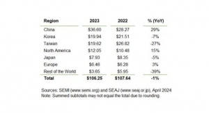
The global semiconductor packaging materials market will track chip industry growth to expand from $17.6 billion in revenue logged in 2019 to $20.8 billion in 2024, a 3.4% CAGR), SEMI and TechSearch International forecast in the Global Semiconductor Packaging Materials Outlook.
A number of semiconductor industry growth drivers will power the surge including big data, high-performance computing (HPC), artificial intelligence (AI), edge computing, advanced memory, the 5G infrastructure build-out, 5G smartphone adoption, growth of electric vehicle adoption and enhanced safety features for automobiles.
Packaging materials are key to the growth of these applications, enabling advanced packaging technologies that undergird the higher performance, reliability and integration of next-generation chips.
Laminate substrates, the largest materials segment, will see a CAGR of over 5%, driven by demand for system-in-package (SIP) and high-performance devices.
Wafer-level packaging (WLP) dielectric will register the highest growth with a 9% CAGR over the forecast period. The trend towards smaller, thinner packaging will dampen the growth of lead frames, die-attach, and encapsulant materials, though new technologies are being developed to enhance performance.
With the steady advance of semiconductor packaging technology innovation, the next several years are expected to present several areas of opportunity in the materials market including:
- New substrate designs to support narrow bump pitch with higher density;
- Low Dk and Df laminate materials for 5G mmWave applications
- Coreless structure based on a modified leadframe technology called Molded Interconnect Solution/System (MIS);
- Mold compounds to provide underfill for copper pillar flip chip;
- Smaller fillers and narrower particle size distribution needed in resin materials to address narrow gaps and fine pitch flip-chip;
- Die attach materials with no-to-low resin bleed, no-to-low outgassing, and processed within <5 µm placement;
- Dielectrics with lower dielectric loss (Df) required for higher frequency applications such as 5G;
- Void-free deposition and low-overburden deposition required for TSV plating
For more information and to purchase the report, visit the SEMI Global Semiconductor Packaging Materials Outlook web page.