09.05.19
Researchers at KU Leuven and imec have successfully developed a new technique to insulate microchips.
The technique uses metal-organic frameworks, a new type of materials consisting of structured nanopores.
In the long term, this method can be used for the development of even smaller and more powerful chips that consume less energy.
The team has received an ERC Proof of Concept grant to further their research.
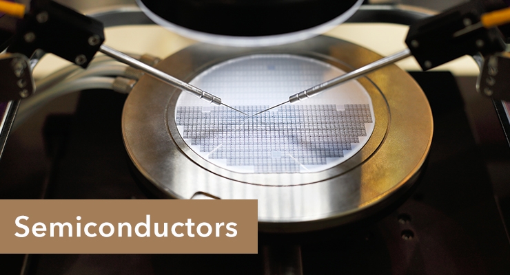
Chips are getting smaller and their processing power is increasing.
Nowadays, a chip can have over a billion transistors.
But this continued reduction in size also brings with it several obstacles. The switches and wires are packed together so tightly that they generate more resistance. This, in turn, causes the chip to consume more energy to send signals. To have a well-functioning chip, one needs an insulating substance that separates the wires from each other and ensures that the electrical signals are not disrupted.
However, that’s not an easy thing to achieve at the nanoscale level.
A study led by KU Leuven professor Rob Ameloot (Department of Microbial and Molecular Systems) shows that a new technique might provide the solution.
“We’re using metal-organic frameworks (MOFs) as the insulating substance," Ameloot said. "These are materials that consist of metal ions and organic molecules. Together, they form a crystal that is porous yet sturdy.”
For the first time, a research team at KU Leuven and imec managed to apply the MOF insulation to electronic material.
An industrial method called chemical vapor deposition was used for this, according to postdoctoral researcher Mikhail Krishtab (Department of Microbial and Molecular Systems).
“First, we place an oxide film on the surface. Then, we let it react with vapor of the organic material. This reaction causes the material to expand, forming the nanoporous crystals," Krishtab said. “The main advantage of this method is that it's bottom-up. We first deposit an oxide film, which then swells up to a very porous MOF material. You can compare it to a soufflé that puffs up in the oven and becomes very light. The MOF material forms a porous structure that fills all the gaps between the conductors. That’s how we know the insulation is complete and homogeneous. With other, top-down methods, there's always still the risk of small gaps in the insulation.”
Prof. Ameloot’s research group has received an ERC Proof of Concept grant to further develop the technique, in collaboration with Silvia Armini from imec’s team working on advanced dielectric materials for nanochips.
“At imec, we have the expertise to develop wafer-based solutions, scaling technologies from lab to fab and paving the way to realizing a manufacturable solution for the microelectronics industry," Armini said.
“We’ve shown that the MOF material has the right properties,” Ameloot said. “Now, we just have to refine the finishing. The surface of the crystals is still irregular at the moment. We have to smoothen this to integrate the material into a chip.”
Once the technique has been perfected, it can be used to create powerful, small chips that consume less energy.
“Various AI applications require a lot of processing power. Think of self-driving cars and smart cities," Ameloot said. "Technology companies are constantly looking for new solutions that are both quick and energy-efficient. Our research can be a valuable contribution to a new generation of chips.”
The technique uses metal-organic frameworks, a new type of materials consisting of structured nanopores.
In the long term, this method can be used for the development of even smaller and more powerful chips that consume less energy.
The team has received an ERC Proof of Concept grant to further their research.
Chips are getting smaller and their processing power is increasing.
Nowadays, a chip can have over a billion transistors.
But this continued reduction in size also brings with it several obstacles. The switches and wires are packed together so tightly that they generate more resistance. This, in turn, causes the chip to consume more energy to send signals. To have a well-functioning chip, one needs an insulating substance that separates the wires from each other and ensures that the electrical signals are not disrupted.
However, that’s not an easy thing to achieve at the nanoscale level.
A study led by KU Leuven professor Rob Ameloot (Department of Microbial and Molecular Systems) shows that a new technique might provide the solution.
“We’re using metal-organic frameworks (MOFs) as the insulating substance," Ameloot said. "These are materials that consist of metal ions and organic molecules. Together, they form a crystal that is porous yet sturdy.”
For the first time, a research team at KU Leuven and imec managed to apply the MOF insulation to electronic material.
An industrial method called chemical vapor deposition was used for this, according to postdoctoral researcher Mikhail Krishtab (Department of Microbial and Molecular Systems).
“First, we place an oxide film on the surface. Then, we let it react with vapor of the organic material. This reaction causes the material to expand, forming the nanoporous crystals," Krishtab said. “The main advantage of this method is that it's bottom-up. We first deposit an oxide film, which then swells up to a very porous MOF material. You can compare it to a soufflé that puffs up in the oven and becomes very light. The MOF material forms a porous structure that fills all the gaps between the conductors. That’s how we know the insulation is complete and homogeneous. With other, top-down methods, there's always still the risk of small gaps in the insulation.”
Prof. Ameloot’s research group has received an ERC Proof of Concept grant to further develop the technique, in collaboration with Silvia Armini from imec’s team working on advanced dielectric materials for nanochips.
“At imec, we have the expertise to develop wafer-based solutions, scaling technologies from lab to fab and paving the way to realizing a manufacturable solution for the microelectronics industry," Armini said.
“We’ve shown that the MOF material has the right properties,” Ameloot said. “Now, we just have to refine the finishing. The surface of the crystals is still irregular at the moment. We have to smoothen this to integrate the material into a chip.”
Once the technique has been perfected, it can be used to create powerful, small chips that consume less energy.
“Various AI applications require a lot of processing power. Think of self-driving cars and smart cities," Ameloot said. "Technology companies are constantly looking for new solutions that are both quick and energy-efficient. Our research can be a valuable contribution to a new generation of chips.”