• Login
    • Join
  • FOLLOW:
  • Subscribe Free
    • eNewsletter
    Checkout
    • Magazine
    • News
    • Printed Electronics
    • Raw Materials
    • Equipment
    • Services
    • Suppliers Guide
    • Resources
    • More
  • Magazine
  • News
  • Printed Electronics
  • Raw Materials
  • Equipment
  • Services
  • Suppliers Guide
  • Resources
  • Current & Past Issues
    Features
    Editorials
    Digital Edition
    Subscribe Now
    Advertise Now
    eNewsletter Archive
    Our Team
    Editorial Guidelines
    Breaking News
    Experts Opinion
    Financial News
    Manufacturers News
    Mergers and Acquisitions
    Online Exclusives
    Personnel
    Product Releases
    Suppliers News
    Live From Shows
    Displays and Lighting
    Photovoltaics
    Printed Batteries
    Printed Circuit Boards/Membrane Switches/In Mold Electronics
    Flexible and Printed Electronics
    RFID and NFC
    Sensors and Wearables
    Smart Cards and Packaging
    Touch Screens
    Adhesives, Barriers and Encapsulants
    Chemicals, Metals and Powders
    Conductive Inks and Coatings
    Electronic Materials
    Film, Paper, Glass and Substrates
    Graphene, Perovskites and Carbon Nanotubes
    Nanomaterials
    Printed Electronic Components
    Research Reports
    Semiconductors and Quantum Dots
    Energy Curing Equipment
    Lab and Testing Equipment
    Manufacturing Equipment
    Printing Equipment
    3D Printing
    Contract Manufacturing Services
    Product Design and Testing
    Research and Consulting
    Research Institutions
    Research Reports
    Universities
    Equipment
    All Companies
    Materials
    Categories
    Converting
    Printed Electronics Systems
    Associations
    Research and Services
    Used Machinery
    Add New Company
    Industry Events
    Live from show events
    Podcasts
    Videos
    Blogs
    Slideshows
    Infographics
    Webinars
    Whitepapers
    Equipment and Services
    Glossary
    • Magazine
      • Current & Past Issues
      • Features
      • Editorial
      • Columns
      • Digital Edition
      • eNewsletter Archive
      • Editorial Guidelines
      • Subscribe Now
      • Advertise Now
    • Breaking News
    • Suppliers Guide
      • Suppliers Guide
      • Add Your Company
    • Printed Electronics
      • Photovoltaics
      • Printed Batteries
      • Printed Circuit Boards/Membrane Switches/In Mold Electronics
      • Flexible and Printed Electronics
      • RFID and NFC
      • Sensors and Wearables
      • Smart Cards and Packaging
      • Touch Screens
    • Raw Materials
      • Adhesives, Barriers and Encapsulants
      • Chemicals, Metals and Powders
      • Conductive Inks and Coatings
      • Electronic Materials
      • Film, Paper, Glass and Substrates
      • Graphene, Perovskites and Carbon Nanotubes
      • Nanomaterials
      • Semiconductors and Quantum Dots
    • Equipment
      • Energy Curing Equipment
      • Lab and Testing Equipment
      • Manufacturing Equipment
      • Printing Equipment
      • 3D Printing
    • Services
      • Contract Manufacturing Services
      • Product Design and Testing
      • Research and Consulting
      • Research Institutions
      • Research Reports
      • Universities
    • Online Exclusives
    • Slideshows
    • Blog
    • Videos
    • Podcasts
    • Infographics
    • Events
      • Industry Events
      • Live from show events
      • Webinars
    • About Us
      • About Us
      • Contact Us
      • Advertise With Us
      • Privacy Policy
      • Terms of Use
    Blog

    imec: Decade of R&D Establishes Europe in Thin-film PV

    An overview of imec’s contributions to a decade of thin-film-PV research and how this fits in the bigger picture.

    imec: Decade of R&D Establishes Europe in Thin-film PV
    Multi-junction PV devices – in this case, a tandem cell of perovskite on top of Si – allow to optimally cover the solar spectrum and increase the energy conversion rates of the overall system.
    Tom Aernouts and Jef Poortmans, R&D Manager of Thin-Film PV, imec and imec Fellow and the Program Director of the Energy activities of imec03.31.21

    In a highly competitive global PV market, Europe remains at the forefront of research and development into next-generation technologies and systems, such as thin-film photovoltaics.


    Thin-film PV technology has been around since the mid-20th Century (in solar-powered calculators, for example). They were rightly considered the lower-efficiency, yet cheaper, the equivalent of conventional Si-PV for a long time. Meanwhile, thanks to multi-junction devices, their efficiencies are competing with (and at lab-scale even surpassing) those of Si-PV. For example, thin-film PV technologies, such as copper indium gallium diselenide (CIGS), have become an established solution in iconic buildings with building-integrated PV (BIPV). 


    Over the past decades, imec has been a key player on the forefront of technology innovations that have brought thin-film PV to its current state-of-the-art and on the verge of conquering the market.


    Thin-film PV is already being used for building-integrated PV in iconic buildings. Left: City of Music, Paris, Shigeru Ban architects, BIPV by ISSOL | Middle: French Ministry of Defense, Paris, ANMA architects, BIPV by ISSOL (©Agence Nicolas Michelin & Associes) |Right: Finance Tower, Liège BE, Jaspers Eyers architects, BIPV by ISSOL ©P.Andrianopoli (Pictures: Courtesy of ISSOL).


    In terms of market share, the big breakthrough of thin-film PV has yet to happen but might be nearer than ever before because of the drive to near-zero-energy buildings and local energy communities. 


    The last decade has brought numerous advances in thin-film R&D, allowing it to start proving its value on a larger scale, especially in integrated-PV solutions such as buildings, vehicles, agri-PV, and others. As a kind of paradox, the dominant Si-PV market might provide the ideal jumping board for thin-film to close in on the top position.


    Combining the best of both worlds: Si-thin-film tandem devices

    The PV-market has grown at a breathtaking rate over the last two decades resulting in a market size that is a thousand times larger than twenty years ago and reaching an installation volume of over 100GWp/year in 2019, which was equivalent to a yearly turnover in the range of $150 billion.


    Although the exact growth scenario remains to be seen, there are sufficient elements to believe that, due to its cost-effectiveness and distributed character, further growth of the PV-sector by a factor of ten in the next two decades is highly probable. 


    In this ambition, performance increase remains critical more than ever before. The present evolution of PV-system prices and their composition often results in an erroneous conclusion. Given that nowadays, the price components related to cell and module manufacturing no longer dominate the total cost, many conclude that it is no longer relevant to look at the PV-cell and module level. 


    This conclusion is, however, totally incorrect. The best way to reduce the weight of all the peripheral and adjacent components such as wires, switches, inverters (aka balance-of-system, or BOS, components) is to increase the number of Wp/m2 or ultimately kWh/m2.


    Since crystalline Si-cells are approaching their practical limit in terms of energy conversion (implied by physical laws), the objective of a performance enhancement can only be achieved when moving towards tandem and ultimately triple-junction configurations; to go over the 30% limit and aim at 35% on cell level. In such multiple-junction systems, various electroactive materials are stacked that have complementary sensitivities within the solar spectrum. Combined, they make more optimal use of the available spectrum and thereby increase the conversion rate of the overall system.


    The type and variety of available materials in thin-film PV allow for optimally tuning each subcell's bandgaps within the tandem, so they cover complementary parts of the solar spectrum. Also, thin-film solutions are lightweight, flexible, and relatively cheap to produce. 


    Because of these inherent characteristics, thin-film technologies are ideally suited to act as the additional layers in traditional Si-PV stacks and, as such, augment them. By doing so, thin-film technologies can optimally take advantage of the existing market scale to further lower their production cost. Moreover, this economy of scale will help to develop the size of the niche markets for products that are purely based on thin-film PV (e.g., vehicle-integrated PV).


    Opportunities for Europe

    The largest part of the PV cell and PV module manufacturing capacity is presently located in Asia and concentrated in China and Malaysia. Although the heart of a PV system is obviously the PV cell, the PV module today represents less than 30% of the PV system's final value in the value chain. It’s important to emphasize that on materials level (encapsulants, glass, metals), balance-of-system (BOS) components, design, installation, operations and maintenance, decommissioning, and recycling/reuse… European companies take a significant part in value creation and are innovation leaders.


    The same holds for thin-film technologies, where tight collaborations within the value chain are even more critical because of the ambitions in terms of integration and mass-customization. 


    Because thin-film technologies require tight integration with conventional PV processing or need to meet the customization requirements of specific end applications in terms of dimensions, shape, and transparency (think of integration in buildings), there will be enormous value in having a coherent production ecosystem as close as possible to the location where the final system needs to be applied. Be it a building-integrated solution (BIPV), in-vehicle integration (VIPV), or the like.


    And it’s precisely on this aspect of tight collaboration and ecosystem coordination that Europe can deploy its proven strengths.


    Building-integrated photovoltaics (BIPV) façade developed within the EU-funded project PVme.


    Imec’s track record in thin-film PV

    One of the proof points of Europe’s strength in R&D collaboration is Solliance, a Solar Research Alliance that since its foundation in 2010 (by TNO, ECN, Holst Centre, TU Eindhoven, and UHasselt) plays a leading role in the worldwide research and development of thin-film solar technology. 


    Imec joined the Netherlands-based initiative as one of the pioneers shortly after the official start and has since worked closely with TNO and the Solliance academic partners to push the boundaries of thin-film PV. Another prime example is EnergyVille, a collaboration between the Belgian research partners KU Leuven, VITO, imec, and UHasselt in sustainable energy and intelligent energy systems. 


    A brand-new lab for thin-film-PV development and upscaling was opened at the EnergyVille-site in 2018, which enormously increased the group's impact in paving the way to upscaling, PV-module making, and stability studies under controlled or outdoor conditions. The efforts on materials development and characterization at IMOMEC, an imec research laboratory at UHasselt, should also not be overlooked.


    Together, these collaborations formed the solid foundation in a field that was substantially disrupted by the appearance of a new group of materials: perovskites.


    Until a decade ago, one of the main activities in the thin-film R&D domain was on organic photovoltaics (OPV): thin-film technologies that use organic compounds as semiconductor material. Since then, perovskites – a specific group of hybrid organic-inorganic materials – have wholly disrupted the field and dominated the thin-film PV domain. They are by far the prime candidate to guarantee the basic efficiency of thin-film solutions, be it still in combination with other materials such as CIGS to realize the beforementioned multi-junction devices.


    Thanks to the available knowledge and collaborations named above, the move from OPV towards perovskites turned out to be particularly successful in terms of results obtained on upscaled devices. As it happened, the processing equipment and conditions required for perovskite-based systems were similar enough to the ones for OPV, allowing Solliance to build on two decades of R&D that imec and other partners had been building on OPV and other advanced thin-film PV technologies. For example, techniques such as spray coating and evaporation developed for OPV and other thin-film flavors proved to be compatible with perovskites after relatively minor tuning of the material stacks, equipment, and processing conditions. 


    As a result, imec/EnergyVille, together with the Dutch partners in the Solliance collaboration, achieved globally leading results, such as the world’s first officially certified large-area perovskite module and several world records in the energy efficiency of thin-film PV cells and systems. Aside from these efforts and achievements on materials and cells, imec and its partners also deploy activities on the adjacent competencies. 


    For example, at EnergyVille focus lies on the topics that are covering the entire value chain from material to (Integrated) PV system. Starting from the vision that Europe can differentiate itself in terms of customization, integration, and the related flexibility in manufacturing conditions, for example, research is conducted on dedicated interconnect solutions that allow for flexibly interconnecting individual (thin-film) PV cells into modules with a diversity of shapes and dimensions. 


    Also, components and systems such as inverters and other peripheral electronics are being investigated in terms of how they can evolve to comply with the specific requirements of PV implementations with a higher degree of customization than what exists in today’s relatively standardized Si-PV implementations.


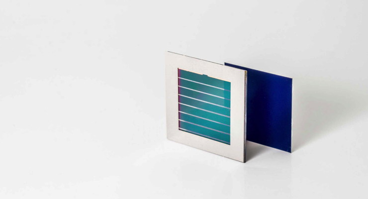
    World’s first demonstration by Solliance partners TNO, imec/EnergyVille and TU/Eindhoven of encapsulated perovskite solar modules fabricated using industrial processes that withstand three established lifetime tests. (image © nielsvanloon.com/photography).


    Throughout all of these activities – from materials, equipment and processes, over module and system integration up to final implementation – the active involvement of industrial partners and the support from national and European public funding cannot be overestimated. On the very basis, the expertise of materials and equipment suppliers allowed rapid adaptation at the disruptive and exciting times when perovskites gained a reputation. 


    Further down the road, glass manufacturers, building, and automotive companies' input and active involvement proved vital to develop suitable solutions for BIPV, VIPV, and other customized applications. And the combination of private and public funding allows for being involved at the forefront of innovation across the thin-film PV domain's full width. 


    Looking back on the past decade's results and looking around at all the stakeholders and ingredients that are continuously growing in their maturity as a well-oiled ecosystem, one can only be enthusiastic and ambitious on where this can bring us in the decade to come. May it act as a warm welcome to everyone involved to maintain or increase their efforts or join in on the adventure for those who haven’t already.

    Suggested For You
    Sogegross Group Increases Productivity with Zebra Technologies Sogegross Group Increases Productivity with Zebra Technologies
    Flex Joins World Economic Forum Flex Joins World Economic Forum
    Metalcraft Launches Inlay Innovation for RFID Inlay Design, Fabrication Metalcraft Launches Inlay Innovation for RFID Inlay Design, Fabrication
    ASSA ABLOY to Acquire HHI Division of Spectrum Brands ASSA ABLOY to Acquire HHI Division of Spectrum Brands
    Applied Materials Develops New Technologies for Silicon Carbide Chipmakers Applied Materials Develops New Technologies for Silicon Carbide Chipmakers
    Zebra Circular Economy Program Honored with Sustainability Service of the Year Zebra Circular Economy Program Honored with Sustainability Service of the Year
    Empa Sets New Record Efficiency for Flexible Solar Cells Empa Sets New Record Efficiency for Flexible Solar Cells
    Powercast’s RF Wireless Power Technology Awarded for Global Sustainability Powercast’s RF Wireless Power Technology Awarded for Global Sustainability
    Pusan University Researchers Develop ‘Super-Flexible’ Electroluminescent Devices for Wearables Pusan University Researchers Develop ‘Super-Flexible’ Electroluminescent Devices for Wearables
    New Partnership Set to Future Proof Process Manufacturing in Scotland New Partnership Set to Future Proof Process Manufacturing in Scotland
    ‘Smart’ Shirt Using Carbon Nanotube Threads Keeps Tabs on the Heart ‘Smart’ Shirt Using Carbon Nanotube Threads Keeps Tabs on the Heart
    Space Mission Tests NREL Perovskite Solar Cells Space Mission Tests NREL Perovskite Solar Cells
    Synaptics to Acquire Chipset Specialist DSP Group Synaptics to Acquire Chipset Specialist DSP Group
    PPG, Universal Display Expand OLED Operations in Ireland PPG, Universal Display Expand OLED Operations in Ireland
    Combining Perovskite with Silicon, Solar Cells Convert More Energy From Sun Combining Perovskite with Silicon, Solar Cells Convert More Energy From Sun

    Related Breaking News

    • Breaking News | Manufacturers News | RFID and NFC
      Sogegross Group Increases Productivity with Zebra Technologies

      Sogegross Group Increases Productivity with Zebra Technologies

      Italian food wholesaler deploys VisibilityIQ Foresight for real-time actionable business insights.
      09.20.21

    • Breaking News | Contract Manufacturing/Printing | Flexible and Printed Electronics | Manufacturers News
      Flex Joins World Economic Forum

      Flex Joins World Economic Forum

      CEO Revathi Advaithi now a member of the Alliance of CEO Climate Leaders.
      09.17.21

    • Breaking News | RFID and NFC
      Metalcraft Launches Inlay Innovation for RFID Inlay Design, Fabrication

      Metalcraft Launches Inlay Innovation for RFID Inlay Design, Fabrication

      Custom RFID inlays from prototype to production ‘Made in USA’ for converters, manufacturers, distributors and integrators.
      09.13.21


    • Breaking News | Manufacturers News | Mergers and Acquisitions | RFID and NFC
      ASSA ABLOY to Acquire HHI Division of Spectrum Brands

      ASSA ABLOY to Acquire HHI Division of Spectrum Brands

      Key brands include Kwikset, Baldwin, Weiser, Pfister and National Hardware.
      09.09.21

    • Breaking News | Displays and Lighting | Semiconductors and Quantum Dots | Suppliers News
      Applied Materials Develops New Technologies for Silicon Carbide Chipmakers

      Applied Materials Develops New Technologies for Silicon Carbide Chipmakers

      Silicon carbide chips are transitioning to larger, 200mm wafers which boost output to meet growing global demand.
      09.09.21

    Loading, Please Wait..
    Trending
    • SCHOTT Strengthens Glass Substrate Portfolio
    • Fujifilm Completes Acquisition Of Electronic Chemicals Business From Entegris
    • Ink-Borne ‘Chiplets’ Could Lead To Printable Displays, Electronics And More
    • Nano Dimension Shareholders Re-Elect All Company Director Nominees
    • Printed Electronics Industry Shows Capabilities During Drupa 2016
    Breaking News
    • Walmart CEO Doug McMillon to Keynote CES 2024
    • JDI Launches Launch Large-Scale eLEAP Project in China
    • Two Scientific Leaders from ORNL Invited to White House Workshop
    • CSEM Appoints Sara Girardi New CFO
    • Fujifilm Completes Acquisition of Electronic Chemicals Business from Entegris
    View Breaking News >
    CURRENT ISSUE

    Winter 2021

    • Printed Electronics Now’s International Suppliers’ Directory
    • The Automotive Market and Flexible and Printed Electronics
    • Flexible and Printed Electronics in Healthcare
    • Flexible and Printed Electronics Make Gains in Smart Packaging
    • PAPERONICS: Low-cost multisensory paper and packaging applications
    • View More >

    Cookies help us to provide you with an excellent service. By using our website, you declare yourself in agreement with our use of cookies.
    You can obtain detailed information about the use of cookies on our website by clicking on "More information”.

    • About Us
    • Privacy Policy
    • Terms And Conditions
    • Contact Us

    follow us

    Subscribe
    Nutraceuticals World

    Latest Breaking News From Nutraceuticals World

    Eriomin Associated with Improved Microbiota in People with Prediabetes
    BAPP Publishes Lab Guidance Document on Lavender Oil
    Bartek Provides Update on Construction of World's Largest Malic, Fumaric Acid Facility
    Coatings World

    Latest Breaking News From Coatings World

    Dunn-Edwards Names ‘Skipping Stones’ 2024 Color of the Year
    PPG Partners with Prague Crafts Academy to Train Next Generation of Painters
    RPM Acquires Leading Panelized Wall Systems Business
    Medical Product Outsourcing

    Latest Breaking News From Medical Product Outsourcing

    Insulet Begins Search for New CFO
    Phillips-Medisize, GlucoModicum Team Up on Needle-Free CGM
    Cadence Inc. Acquires Florida Location of ARC Group Worldwide
    Contract Pharma

    Latest Breaking News From Contract Pharma

    Emmes Appoints Matt Bond CFO
    PTC Furthers Workforce Reduction
    PharmaEssentia, WuXi Biologics Ink Exclusive Global License Agreement
    Beauty Packaging

    Latest Breaking News From Beauty Packaging

    Thrive Causemetics Launches ‘Sheryl’ Lipstick to Honor Find Your Fabulosity Founder
    Maesa Names Winners of First Ever Magic Incubator
    L'Oréal Sells Certified-Organic Beauty Brand Sanoflore
    Happi

    Latest Breaking News From Happi

    Clearstem Skincare Introduces First Acne Lab Test
    Wellness Brand Agent Nateur's Launch With Vitamin Shoppe Takes Manhattan
    Thrive Causemetics Creates Lipstick Shade to Honor Find Your Fabulosity CEO Sheryl Kurland
    Ink World

    Latest Breaking News From Ink World

    Inkcups to Showcase Portfolio at PRINTING United 2023
    Koenig & Bauer Factory in Radebeul Celebrates Its Jubilee
    Fraunhofer IPA Creates Pigments from Crustaceans
    Label & Narrow Web

    Latest Breaking News From Label & Narrow Web

    All Printing Resources partners with MicroDynamics
    IST America to make Printing United debut
    Sun Chemical’s Glenn Webster receives NAPIM award
    Nonwovens Industry

    Latest Breaking News From Nonwovens Industry

    Conwed Refreshes Branding, Website
    Registration Opens for 2024 ACI Convention
    RISE Conference Held at NC State
    Orthopedic Design & Technology

    Latest Breaking News From Orthopedic Design & Technology

    Loci Ortho Completes Enrollment for THANKS Clinical Trial
    Augmedics Hires Medtronic AI Expert as VP of R&D
    SurGenTec Introduces TiLink-P Sacroiliac Joint Compression Implant
    Printed Electronics Now

    Latest Breaking News From Printed Electronics Now

    Walmart CEO Doug McMillon to Keynote CES 2024
    JDI Launches Launch Large-Scale eLEAP Project in China
    Two Scientific Leaders from ORNL Invited to White House Workshop

    Copyright © 2023 Rodman Media. All rights reserved. Use of this constitutes acceptance of our privacy policy The material on this site may not be reproduced, distributed, transmitted, or otherwise used, except with the prior written permission of Rodman Media.

    AD BLOCKER DETECTED

    Our website is made possible by displaying online advertisements to our visitors.
    Please consider supporting us by disabling your ad blocker.


    FREE SUBSCRIPTION Already a subscriber? Login