07.09.18
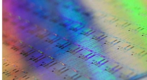
At its annual Imec Technology Forum USA in San Francisco, imec, in collaboration with Soitec, a leader in the design and production of innovative semiconductor materials for the electronics industry, reported that they successfully demonstrated a sequential 3D front-end integration process by stacking two device layers on one another on a 300mm wafer.
This vertical integration of sequentially processed device layers, also named sequential-3D integration (S3D), is perceived as a promising alternative to continue the benefits offered by semiconductor scaling, overcoming the constraints of geometrical scaling while maintaining the benefits of functional scaling through the vertical 3D integration.
The most critical challenge of sequential-3D integration is the management of the fabrication thermal budget. To avoid or limit thermally induced device degradation issues of the bottom device layer, the top device layer must be processed at low temperatures below 525°C. The top thermal budget needs to be reduced to avoid degradation of the bottom devices, the bottom interconnects, and the bonding interface. These limitations are overcome with the implementation of junction-less transistors on the top-layer which decreases the fabrication complexity and provides sufficient device reliability.
A high device density per chip area can be realized because the alignment accuracy only depends on the lithography stepper performance and not on the accuracy of the wafer alignment, as is the case for alternative 3D-integration technologies using through-Si vias.
For efficient sequential device stacking, imec worked with Soitec’s Smart Cut technology to transfer a thin layer of crystalline material from one substrate to the substrate processed with the first layer of devices, overcoming physical limitations and opening innovative opportunities in 3D IC product design.
“This exciting R&D collaboration between imec and Soitec is paving the way for global innovation,” said Bich-yen Nguyen, senior fellow at Soitec.