09.29.23
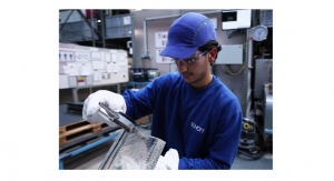
SCHOTT is taking steps to support the integrated circuit (IC) industry in advancing the pace of Moore's Law with new materials. This development is needed for more powerful computing intended for applications such as artificial intelligence (AI). As uncompromised, high-quality glass substrates are crucial for enabling advanced packaging in the upcoming decade, SCHOTT is proactively setting the course to enable the industry to innovate even further.
The future of chip packaging starts with glass. SCHOTT CEO Dr. Frank Heinricht underlines the company's commitment to the IC industry, while highlighting the steps already taken to handle increasing demand.
“Today, we are announcing a three-point action plan to tackle the increasing demand for glass substrates for advanced packaging. Our action plan is broken up into three points of focus: researching, upgrading, and investing,” said Dr. Heinricht. “As we have been in a constant exchange with industry leaders, we are now accelerating our product development and have already established a leading position to immediately supply high-quality substrates the chip industry's R&D teams need."
The action plan addresses the following glass substrate-related areas that have a direct impact on chip packaging designs and markets:
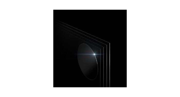
1. Product innovations: Major SCHOTT material innovations for a diverse range of applications targeting the IC industry are already available to customers today. Additionally, unique substrates that are tailor-made for diverse applications in advanced chip packaging have entered the final stage of market-readiness.
2. Upgrading of existing substrates: Over the past years, glass substrate innovations tar-geting the IC industry have undergone constant optimization and development, e.g., by regularly improving geometric tolerances, securing exceptional flatness, and adding max-imum versatility in format, thickness range, and material development on various characteristics. SCHOTT will continue this orientation to be ready for the industry requirements.
3. Expansion of melting and processing capacities and capabilities: With increasing demand, large-scale level capacities are needed to supply seamlessly. SCHOTT has already decided to expand its infrastructure to brace the rise of the industry. For example, capaci-ties and capabilities of SCHOTT’s facilities in Europe and Asia will be continuously extended.
"Major steps in advanced packaging can be realized based on material innovations. As glass offers numerous attributes that have clear benefits for semiconductor manufacturing, specialty glass has the potential to bring advanced packaging to the next level," said Stefan Hergott, head of SCHOTT's Special Flat Glass & Wafer unit.
Unique properties of glass, such as thermal, mechanical properties, or an ultra-low flatness in geometrical property, are trailblazing innovation and new products in semiconductor packaging. Therefore, these attributes enable semicon experts to create high-end packaging with a much higher performance and more flexibility.
Besides the most recent innovations in the field of glass substrates tailored for the semiconductor industry, SCHOTT's products have been a key part of the chip manufacturing industry for decades as well. The near-zero expansion material ZERODUR, for example, is a crucial component of leading lithography machines worldwide.
Within these lithography machines, silicon wafers and exposure masks must be positioned precisely to produce the finest structures for the most potent microchips. SCHOTT products, including flexible light guides, ensure that the highest precision is maintained during the process. Since these machines are used in all chip foundries and IDMs around the world, nearly all computer chips on earth encounter specialty glass from SCHOTT.
The future of chip packaging starts with glass. SCHOTT CEO Dr. Frank Heinricht underlines the company's commitment to the IC industry, while highlighting the steps already taken to handle increasing demand.
“Today, we are announcing a three-point action plan to tackle the increasing demand for glass substrates for advanced packaging. Our action plan is broken up into three points of focus: researching, upgrading, and investing,” said Dr. Heinricht. “As we have been in a constant exchange with industry leaders, we are now accelerating our product development and have already established a leading position to immediately supply high-quality substrates the chip industry's R&D teams need."
The action plan addresses the following glass substrate-related areas that have a direct impact on chip packaging designs and markets:
1. Product innovations: Major SCHOTT material innovations for a diverse range of applications targeting the IC industry are already available to customers today. Additionally, unique substrates that are tailor-made for diverse applications in advanced chip packaging have entered the final stage of market-readiness.
2. Upgrading of existing substrates: Over the past years, glass substrate innovations tar-geting the IC industry have undergone constant optimization and development, e.g., by regularly improving geometric tolerances, securing exceptional flatness, and adding max-imum versatility in format, thickness range, and material development on various characteristics. SCHOTT will continue this orientation to be ready for the industry requirements.
3. Expansion of melting and processing capacities and capabilities: With increasing demand, large-scale level capacities are needed to supply seamlessly. SCHOTT has already decided to expand its infrastructure to brace the rise of the industry. For example, capaci-ties and capabilities of SCHOTT’s facilities in Europe and Asia will be continuously extended.
"Major steps in advanced packaging can be realized based on material innovations. As glass offers numerous attributes that have clear benefits for semiconductor manufacturing, specialty glass has the potential to bring advanced packaging to the next level," said Stefan Hergott, head of SCHOTT's Special Flat Glass & Wafer unit.
Unique properties of glass, such as thermal, mechanical properties, or an ultra-low flatness in geometrical property, are trailblazing innovation and new products in semiconductor packaging. Therefore, these attributes enable semicon experts to create high-end packaging with a much higher performance and more flexibility.
Besides the most recent innovations in the field of glass substrates tailored for the semiconductor industry, SCHOTT's products have been a key part of the chip manufacturing industry for decades as well. The near-zero expansion material ZERODUR, for example, is a crucial component of leading lithography machines worldwide.
Within these lithography machines, silicon wafers and exposure masks must be positioned precisely to produce the finest structures for the most potent microchips. SCHOTT products, including flexible light guides, ensure that the highest precision is maintained during the process. Since these machines are used in all chip foundries and IDMs around the world, nearly all computer chips on earth encounter specialty glass from SCHOTT.