• Login
    • Join
  • FOLLOW:
  • Subscribe Free
    • eNewsletter
    Checkout
    • Magazine
    • News
    • Printed Electronics
    • Raw Materials
    • Equipment
    • Services
    • Suppliers Guide
    • Resources
    • More
  • Magazine
  • News
  • Printed Electronics
  • Raw Materials
  • Equipment
  • Services
  • Suppliers Guide
  • Resources
  • Current & Past Issues
    Features
    Editorials
    Digital Edition
    Subscribe Now
    Advertise Now
    eNewsletter Archive
    Our Team
    Editorial Guidelines
    Breaking News
    Experts Opinion
    Financial News
    Manufacturers News
    Mergers and Acquisitions
    Online Exclusives
    Personnel
    Product Releases
    Suppliers News
    Live From Shows
    Displays and Lighting
    Photovoltaics
    Printed Batteries
    Printed Circuit Boards/Membrane Switches/In Mold Electronics
    Flexible and Printed Electronics
    RFID and NFC
    Sensors and Wearables
    Smart Cards and Packaging
    Touch Screens
    Adhesives, Barriers and Encapsulants
    Chemicals, Metals and Powders
    Conductive Inks and Coatings
    Electronic Materials
    Film, Paper, Glass and Substrates
    Graphene, Perovskites and Carbon Nanotubes
    Nanomaterials
    Printed Electronic Components
    Research Reports
    Semiconductors and Quantum Dots
    Energy Curing Equipment
    Lab and Testing Equipment
    Manufacturing Equipment
    Printing Equipment
    3D Printing
    Contract Manufacturing Services
    Product Design and Testing
    Research and Consulting
    Research Institutions
    Research Reports
    Universities
    Equipment
    All Companies
    Materials
    Categories
    Converting
    Printed Electronics Systems
    Associations
    Research and Services
    Used Machinery
    Add New Company
    Industry Events
    Live from show events
    Podcasts
    Videos
    Blogs
    Slideshows
    Infographics
    Webinars
    Whitepapers
    Equipment and Services
    Glossary
    • Magazine
      • Current & Past Issues
      • Features
      • Editorial
      • Columns
      • Digital Edition
      • eNewsletter Archive
      • Editorial Guidelines
      • Subscribe Now
      • Advertise Now
    • Breaking News
    • Suppliers Guide
      • Suppliers Guide
      • Add Your Company
    • Printed Electronics
      • Photovoltaics
      • Printed Batteries
      • Printed Circuit Boards/Membrane Switches/In Mold Electronics
      • Flexible and Printed Electronics
      • RFID and NFC
      • Sensors and Wearables
      • Smart Cards and Packaging
      • Touch Screens
    • Raw Materials
      • Adhesives, Barriers and Encapsulants
      • Chemicals, Metals and Powders
      • Conductive Inks and Coatings
      • Electronic Materials
      • Film, Paper, Glass and Substrates
      • Graphene, Perovskites and Carbon Nanotubes
      • Nanomaterials
      • Semiconductors and Quantum Dots
    • Equipment
      • Energy Curing Equipment
      • Lab and Testing Equipment
      • Manufacturing Equipment
      • Printing Equipment
      • 3D Printing
    • Services
      • Contract Manufacturing Services
      • Product Design and Testing
      • Research and Consulting
      • Research Institutions
      • Research Reports
      • Universities
    • Online Exclusives
    • Slideshows
    • Blog
    • Videos
    • Podcasts
    • Infographics
    • Events
      • Industry Events
      • Live from show events
      • Webinars
    • About Us
      • About Us
      • Contact Us
      • Advertise With Us
      • Privacy Policy
      • Terms of Use
    Expert's Opinion

    imec: Revolutionizing Material Characterization to Support Future Semiconductor Device Fabrication

    Table-top high-harmonic generation sources feeding industry-relevant characterization needs.

    imec: Revolutionizing Material Characterization to Support Future Semiconductor Device Fabrication
    Paul van der Heide, Director of the MCA department & Co-AttoLab Principal at imec03.24.21
    The emergence of new materials to support semiconductor device scaling drives new characterization needs. 
     
    Table-top high harmonic generation (HHG) sources feeding advanced imaging and spectroscopy techniques complementing those found at synchrotron sites are being examined as a potential source to fill these needs.
     
    This is the beating heart of the AttoLab, a game-changing, multifunctional characterization facility initiated by imec in collaboration with KMLabs and SPECS.
     
    Materials characterization/metrology are key enablers in the semiconductor industry as they not only support fundamental R&D but also provide a means to ensure that high volume manufacturing (HVM) is proceeding as spec’d. And with Moore’s law continuing its relentless path forward (3nm logic process flows are expected to go into production mid-2022/early 2023 with 2nm due shortly thereafter), the question is: how small can we go?
     
    One of the barriers to further downscaling concerns electrical leakage in the form of short channel effects. To contend with this, novel new solid-state materials and architectures are continuously being explored.
    And with this, 2D materials, which include graphene, transition metal dichalcogenides (TMDs) and topological insulators (TIs), are now appearing on various technology roadmaps. That means the needed R&D needs to happen now.
     
    2D materials are of interest since they display attractive carrier mobilities along with reduced leakage issues. Graphene (a 2D carbon allotrope) for example, may potentially be used in future logic devices (carbon-nano-ribbons open a bandgap), memory devices, optoelectronic devices and/or interconnects. As for TMDs, examples such as tungsten disulfide (WS2) and molybdenum disulfide (MoS2) are being looked at as potential replacements of silicon (Si) in the conduction channel of logic devices as well as optoelectronic devices. And like graphene, TMDs can be arranged as multi or mono-layer structures.
     
    And lastly, much is anticipated from 3D topological insulators (TIs), a material class that was first theorized in 2005 and for which the 2016 Nobel Prize in Physics was awarded. 3D-TIs behave like an insulator in their interior, but their surface contains spin-locked conductive states, i.e., all electrons traveling in a given direction will have the same spin. Furthermore, these will be protected from defect scattering. Along with potential applications in logic and memory devices realized, TIs may also provide a means to de-coherence-free quantum computing with the bismuth selenide (Bi2Se3) form taking center stage, at least for the moment.


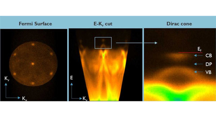
    The unique properties of TIs stem from their topological properties or more precisely, the existence of “Dirac points” in their electronic band structures. These “Dirac points” are formed at energy levels near the Fermi edge and take the shape of the upper (conduction) and lower (valence) halves of a conical surface, hence are referred to as “Dirac cones."

    The performance of any electronic device reliant on atomic-scale engineering is governed by such things as chemical composition inclusive of dopant levels within the respective films as well as interface quality. And the continued downscaling is pushing the limits of what is possible with existing characterization capabilities, whether used in the lab or the fab.


    Today, lab-based solid-state characterization is mainly centered around the imaging techniques of scanning electron microscopy (SEM), transmission electron microscopy (TEM) and those within the scanning probe microscopy (SPM) family inclusive of atomic force microscopy (AFM). There is also a plethora of spectroscopic and spectrometric techniques used such as: infra-red (IR), Raman, x-ray photoelectron spectroscopy (XPS) and variants thereof, Rutherford backscattering (RBS), secondary ion mass spectroscopy (SIMS), atom probe tomography (APT), and the list goes on.


    2D materials, however, bring new analytical requirements and challenges, with examples including being able to measure electron spin, magnetism, and the electron band structure.


    Time-resolved (tr) techniques will also be needed to understand the dynamics of such things as electron spin flipping as this plays a central role in spintronics-based devices.


    With this, and interference lithography in mind, imec started in 2019 a joint development project with KMLabs and SPECS to create what is referred to as the “AttoLab.”


    In 2020, two table-top high-harmonic generations (HHG) extreme ultraviolet (EUV) sources fed by a high-powered femtosecond titanium-sapphire laser was made operational. These HHG sources provide bright coherent pulsed photon beams. One of them feeds a table-top imaging/spectroscopy beamline with 25-120 eV (50-10 nm) photons, while the other feeds a table-top EUV interference lithography (EUV-IL) beamline with 92 eV (13.5 nm) photons. An IR spectroscopy end-station was also set up on the imaging/spectroscopy beamline. And lastly, low energy electron diffraction (LEED), angle-resolved photoemission spectroscopy (ARPES) and photoelectron emission microscopy (PEEM) instrumentation were installed.


    Moving forward, the imaging/spectroscopy beamline will be extended to the ARPES/PEEM chamber. This beamline will also support coherence diffractive imaging (CDI) and magneto-optical Kerr effect (MOKE). And lastly, the introduction of pump-probe photon beams will facilitate tr studies. Recognition of the value of tr-IR and tr-ARPES is highlighted by the fact that Kevin Dorney and Dhirendra Pratap Singh were both awarded Marie Skłodowska-Curie Actions grants in 2021 for their AttoSPIE and AttoPES projects.


    In the longer term, additional capabilities ranging from EUV magneto circular dichroism (MCD), MCD-PEEM, MCD-CDI to various forms of scatterometry and reflectometry are foreseen. The eventual vision is to push the limits of HHG sources such that fully coherent ultra-fast pulsed photon beams up to 1.2 keV (1 nm) are realized. This has the potential to drive CDI to nm scale spatial resolution while also enabling the implementation of near-edge x-ray absorption fine structure (NEXAFS), i.e., techniques typically confined to synchrotron sites. This highly accessible table-top facility will thus serve to enhance time-to-data from months to days.


    IR, ARPES and MOKE (in its traditional form), are spectroscopies that are sensitive to valence shell electrons, with IR providing information on molecular structure, ARPES mapping the valence band structure (ARPES was the 1st technique to empirically map Dirac cones in 2007), and MOKE for measuring magnetization. The implementation of tr capabilities, via pump-probe methods, takes these spectroscopies to the next level as this allows for the kinetics to be followed, i.e., the pump-photon induces a change for which the probe photon following a short time later will measure. As an example, pumping electrons into unoccupied levels above the Fermi edge will allow for Floquet-Bloch states among other things, to be examined (this is the topic of the AttoPES tr-ARPES project). 


    Comparison of tr-IR and tr-ARPES spectra with those obtained via ab-initio calculations within imec will thus provide a deeper level of understanding of processes active to femtosecond regimes and beyond.

    Increasing the energy of the incoming photons into the EUV region will allow for the examination of shallow core level electrons via the implementation of EUV-MOKE and EUV-MCD. And since the energies of core electrons scale more closely with the number of protons in the nucleus, this will provide information on the element responsible for magnetization. Indeed, with photon energies up to 120 eV one will be able to probe 1st-row transition metals inclusive of Fe, Co, and Ni. To probe deeper core levels will require even higher energies.


    And with the long-term vision extending to 1.2 keV, this would be realized. 1.2 keV will also facilitate the implementation of NEXAFS, providing detailed information on elemental speciation, i.e., the chemical compound formed.


    As for LEED, PEEM and CDI, the former is a crystallographic technique, while the latter two are imaging techniques. PEEM maps the locations of photoemissions from a solid to a spatial resolution in the 20-100nm range (70nm in the AttoLab system), and thus provides ARPES with the ability to examine a specific region of interest. Likewise, LEED ensures the film of interest has been prepared correctly before PEEM/ARPES experiments (all are within the same instrument). Lastly, CDI relies on the phase shift experienced by a coherent photon beam directed at a solid. This can provide SEM and AFM-like images to a spatial resolution better than PEEM, but not yet in the realm of SEM and AFM (~1 nm for both). And since CDI resolution scales with wavelength, it is of interest to see what can be attained at 1.2 keV (1 nm), while also pushing scatterometry/reflectometry possibilities. 


    And to examine magnetized regions to unprecedented spatial resolution (down to a few nm or less?) one can envisage the application of MCD-PEEM, or even MCD-CDI.


    Recently, the AttoLab team hit one of its first milestones by observing, via ARPES, the Dirac cone in imec fabricated Bi2Se3 topological insulator films. Although Bi2Se3 has potential applications in logic and memory devices, this work was carried out in the context of developing the next generation of de-coherence-free qubits. These qubits, called Majorana qubits, are the subject of the NOTICE project for which imec’s Clement Merckling was awarded a 5-year ERC Consolidator Grant in 2019. The observation of the Bi2Se3 Dirac cone not only proves that the fabricated material behaves like a topological insulator, but will also enable the tailoring and refinement of Bi2Se3 processing. For this proof-of-concept experiment, the He discharge source within the ARPES instrument was operated to provide a continuous source of photons at 21.2 eV.


    Table-top high-harmonic generation sources can enable a variety of imaging and spectroscopic capabilities that will be key for the characterization and fundamental understanding of emerging materials, inclusive of 2D materials. When implemented in an industry-relevant laboratory – such as the AttoLab – they will accelerate the development of next-generation logic, memory and quantum devices. With the first observation via ARPES of a Dirac cone within imec fabricated Bi2Se3 films, the AttoLab is well on course to realize the R&D goals laid out during its inception.

    Suggested For You
    Jabil’s May Yap Awarded 2021 CIO of the Year by IDC Singapore Jabil’s May Yap Awarded 2021 CIO of the Year by IDC Singapore
    Integrated Electronics Trend to Drive In-Mold Electronics to $1.5 Billion by 2032: IDTechEx Integrated Electronics Trend to Drive In-Mold Electronics to $1.5 Billion by 2032: IDTechEx
    The 2021 Conductive Ink Market The 2021 Conductive Ink Market
    Sustainability and the Flexible and Printed Electronics Industry Sustainability and the Flexible and Printed Electronics Industry
    RDS Launches Tianma 13.3-inch Full HD TFT RDS Launches Tianma 13.3-inch Full HD TFT
    SEMI: North American Semiconductor Equipment Posts $3.65 Billion in Billings in August 2021 SEMI: North American Semiconductor Equipment Posts $3.65 Billion in Billings in August 2021
    Sensirion Opens New Sensor Production Site in Hungary Sensirion Opens New Sensor Production Site in Hungary
    Jabil Board of Directors Appoints CEO Mark Mondello as Chairman of the Board Jabil Board of Directors Appoints CEO Mark Mondello as Chairman of the Board
    Sensirion Acquires Machine Diagnostics Start-up AiSight Sensirion Acquires Machine Diagnostics Start-up AiSight
    Sogegross Group Increases Productivity with Zebra Technologies Sogegross Group Increases Productivity with Zebra Technologies
    Flex Receives Third Consecutive European Lenovo Logistics Excellence Award Flex Receives Third Consecutive European Lenovo Logistics Excellence Award
    JOLED Display Adopted for Newly-Announced ASUS OLED Monitor for HDR Content Creators JOLED Display Adopted for Newly-Announced ASUS OLED Monitor for HDR Content Creators
    ams OSRAM to Showcase Sensor Portfolio at Sensors Converge 2021 ams OSRAM to Showcase Sensor Portfolio at Sensors Converge 2021
    eMagin Finalizes $33.6 Million US DoD Contract for OLED Microdisplays eMagin Finalizes $33.6 Million US DoD Contract for OLED Microdisplays
    Seven in 10 Hospital Executives See Need to Invest More to Maximize Staff Efficiency Seven in 10 Hospital Executives See Need to Invest More to Maximize Staff Efficiency

    Related Breaking News

    • Breaking News | Contract Manufacturing/Printing | Flexible and Printed Electronics | Manufacturers News | Personnel
      Jabil’s May Yap Awarded 2021 CIO of the Year by IDC Singapore

      Jabil’s May Yap Awarded 2021 CIO of the Year by IDC Singapore

      Award recognizes her exemplary work in digital transformation.
      09.23.21

    • Manufacturers News | Printed Circuit Boards/Membrane Switches/In Mold Electronics | Research Reports | Suppliers News
      Integrated Electronics Trend to Drive In-Mold Electronics to $1.5 Billion by 2032: IDTechEx

      Integrated Electronics Trend to Drive In-Mold Electronics to $1.5 Billion by 2032: IDTechEx

      Among other applications, IME is an efficient approach to making curved touch-sensitive interfaces.
      IDTechEx 09.22.21

    • Conductive Inks and Coatings | Flexible and Printed Electronics | Manufacturers News | Photovoltaics | Printed Circuit Boards/Membrane Switches/In Mold Electronics | Sensors and Wearables | Smart Cards and Packaging | Suppliers News
      The 2021 Conductive Ink Market

      The 2021 Conductive Ink Market

      The conductive ink industry is growing with new applications on the horizon, but silver prices remain a concern.
      David Savastano, Editor 09.22.21


    • Breaking News | Displays and Lighting | Manufacturers News
      RDS Launches Tianma 13.3-inch Full HD TFT

      RDS Launches Tianma 13.3-inch Full HD TFT

      Designed to meet the demanding requirements of the industrial and medical display markets.
      09.22.21

    • Flexible and Printed Electronics | Manufacturers News | Photovoltaics | Printed Batteries | Sensors and Wearables | Suppliers News

      Sustainability and the Flexible and Printed Electronics Industry

      Flexible and printed electronics does have a good story to tell when it comes to sustainability.
      David Savastano, Editor 09.22.21

    Loading, Please Wait..
    Trending
    • GlobalFoundries, STMicroelectronics Partner On New Facility
    • Printed Electronics Now Interview: Francisco Melo Of Avery Dennison
    • ASSA ABLOY Receives Clearance From Mexico For HHI Acquisition
    • CircEl‐Paper: Recyclable Paper‐Based Electronics
    • With Its Ambient IoT, Wiliot Makes Inroads In IoT
    Breaking News
    • Sensormatic Unveils Sensormatic Synergy Media Display
    • ams OSRAM Receives the German Innovation Award
    • ASSA ABLOY Receives Clearance from Mexico for HHI Acquisition
    • Christoph Ostermann Named Chairman of Heliatek‘s Advisory Board
    • IMI Europe Announces InnoLAE 2024
    View Breaking News >
    CURRENT ISSUE

    Winter 2021

    • Printed Electronics Now’s International Suppliers’ Directory
    • The Automotive Market and Flexible and Printed Electronics
    • Flexible and Printed Electronics in Healthcare
    • Flexible and Printed Electronics Make Gains in Smart Packaging
    • PAPERONICS: Low-cost multisensory paper and packaging applications
    • View More >

    Cookies help us to provide you with an excellent service. By using our website, you declare yourself in agreement with our use of cookies.
    You can obtain detailed information about the use of cookies on our website by clicking on "More information”.

    • About Us
    • Privacy Policy
    • Terms And Conditions
    • Contact Us

    follow us

    Subscribe
    Nutraceuticals World

    Latest Breaking News From Nutraceuticals World

    Sempera Organics and Alkemist Labs Announce Partnership for Mushroom Testing
    Nektium Expands International Distribution Network for Botanical Extracts
    Kemin Receives Positive EFSA Opinion for BetaVia Pure, its Beta-Glucan Ingredient
    Coatings World

    Latest Breaking News From Coatings World

    PPG’s New Paint for a New Start Initiative to Beautify Schools Worldwide with Colorful Makeovers
    Powder Technology, Inc. Announces New Electrical Coating
    Michelman Chosen as Inaugural Recipient of Innovation Research Interchange (IRI) Excellence Award
    Medical Product Outsourcing

    Latest Breaking News From Medical Product Outsourcing

    Bausch + Lomb, Heidelberg Debut Digital Surgical Visualization Platform
    FDA Approves Endologix's Detour System for PAD
    Avanos to Sell Respiratory Health Biz to SunMed
    Contract Pharma

    Latest Breaking News From Contract Pharma

    EUROAPI Invests €50M to Meet Growing Demand for Prostaglandins
    RK Pharma to Receive $200M Investment from PAG
    Axol Bioscience, StrataStem Partner on ‘Clinical Trial in a Dish’ for Alzheimer’s Disease
    Beauty Packaging

    Latest Breaking News From Beauty Packaging

    Beiersdorf Shares Progress of Its Sustainability Agenda
    Estée Lauder Announces Second Edition of Beauty&You Brand Incubator Program
    GetHarley Raises $52 Million in Latest Funding Round
    Happi

    Latest Breaking News From Happi

    Beautycon Returns for 2023 at the Essence Festival of Culture in New Orleans
    Gen Z Entrepreneur Introduces The Ashley Marie Collection for 4C Hair Types
    Carrière Frères Introduces Candle Refills as New Sustainability Initiative
    Ink World

    Latest Breaking News From Ink World

    SICPA Inaugurates Its unlimitrust Campus
    Siegwerk’s Center of Excellence in France Receives Facelift
    Epson announces MakeTheSwitch Campaign
    Label & Narrow Web

    Latest Breaking News From Label & Narrow Web

    Gallus to celebrate 100 years, opening New Gallus Experience Center
    Mark Andy holds successful Low Migration Workshop
    Ryback & Ryback Consulting launches Machinery division
    Nonwovens Industry

    Latest Breaking News From Nonwovens Industry

    Terra Baby Diapers, Wipes Launch in U.S. and Canada
    The Honest Company to Exit Europe, Asia
    TechnoPlants to Exhibit at ITMA
    Orthopedic Design & Technology

    Latest Breaking News From Orthopedic Design & Technology

    European Regulators Approve Amber Implants' VCFix Spinal System Study
    Orthobiologics Market to Top $10.3 Billion by 2030
    Artelon Granted U.S. FDA 510(k) Clearance for FlexBand, FlexPatch & FlexBand Plus
    Printed Electronics Now

    Latest Breaking News From Printed Electronics Now

    Sensormatic Unveils Sensormatic Synergy Media Display
    ams OSRAM Receives the German Innovation Award
    ASSA ABLOY Receives Clearance from Mexico for HHI Acquisition

    Copyright © 2023 Rodman Media. All rights reserved. Use of this constitutes acceptance of our privacy policy The material on this site may not be reproduced, distributed, transmitted, or otherwise used, except with the prior written permission of Rodman Media.

    AD BLOCKER DETECTED

    Our website is made possible by displaying online advertisements to our visitors.
    Please consider supporting us by disabling your ad blocker.


    FREE SUBSCRIPTION Already a subscriber? Login