David Savastano, Editor10.10.18
Developing flexible circuitry is an essential component of flexible hybrid electronics systems. Manufacturers are looking for smaller, more densely packed circuits or their applications, and this is proving to be an ideal opportunity for MicroConnex.
A specialist in commercial flexible circuits fabrication and laser micromachining services, Snoqualmie, WA-based MicroConnex develops high-density flex interconnects (HDI) solutions for the electronic packaging market. The company uses its proprietary photolithographic patterning systems to produce custom flexible circuitry. Key markets include medical ultrasound systems, semiconductor and defense and aerospace industries.
Steve Leith, MicroConnex’s VP engineering and technology, said that MicroConnex was formed as an R&D company called MicroSound Systems in the mid-1990s.
“The initial business concept was to develop next generation, complex medical ultrasound transducers and this early work were partially funded by DARPA and the US Navy,” Leith said. “The company co-founders were experts in ultrasound, but during the course of the project found that the 2D ultrasonic transducers required complex interconnects not readily available from third parties. By necessity they had to develop high-density flex interconnects (HDI) in-house to enable demonstration of the ultrasonic device.
“In developing the skill in fabricating specialty flex circuits, it became clear that the real value proposition of the company wasn’t ultrasonic devices, but fabricating the interconnects required to interface with the mesoscale world,” he added. “The team then created MicroConnex as a technology-centric business focused on high-density flex circuit fabrication leveraging the company expertise in laser micro-machining and thin film deposition.”
The HDI business is highly competitive. MicroConnex is working with the Washington Clean Energy Test Beds (WCET) to overcome the cost vs. performance pressure in the HDI marketplace.
“We believe that we can address a portion of the market needs using a hybrid circuit fabrication process that utilizes elements of printing and electrodeposition; our colleagues at WCET are experts in printing on plastic technology and MicroConnex has a very deep bench in electrodeposition of nano- and micro-scale architectures,” Leith noted. “The idea to combine these two technologies resulted from an assessment of circuit functional requirements vs. available, reasonably mature fabrication processes.”
Leith said that ideal markets for MicroConnex are those that require the smallest and thinnest densely populated flexible circuitry.
“Examples abound in the medical device space in which small and thin circuit design elements are required for functionality,” he reported. “Specifically, electrophysiology (EP) mapping/ablation applications (i.e. cardiac mapping and ablation) are platforms that benefit from HDI circuit technology. Hearing aids (including cochlear implants), vision enhancement devices, drug delivery, and medical ultrasound are other applications in which HDI plays a key role. The motivation for the technology under development is that flex circuits made with the hybrid process may be used to fabrication these types of devices with disruptive performance vs cost metrics.”
One of the biggest challenges has been the ability to use roll-to-roll fabrication techniques. NextFlex is funding MicroConnex’s project to develop a two-step “hybrid” printing process in which fine circuit patterns are first printed using an R2R process.
“In the last 10-15 years, significant resources (people and R&D funds) have been spent trying to solve some fundamental material and processing challenges in R2R printed electronics fabrication,” said Leith. “The technology has evolved and improved based on hard work and wide-ranging contributions by numerous industrial and academic developers around the globe, yet many of the same issues remain. The primary technical challenges include demonstrating adequate adhesion of the printed material to the substrate (does the circuit stick to the plastic), achieving targeted dimensional control of the circuits (how accurately circuit widths and thickness can be controlled) and fabricating circuits with sufficient electrical performance to be useful (primarily high enough conductivity).
“Adhesion is influenced by the chemical and physical attributes of the substrate, the chemical and physical attributes of the printed ‘ink’ that becomes the circuit and the specific process used in ‘rolling’ the ink onto the substrate (think pressure, speed, temperature, roller material, etc.),” Leith continued. “We are working with our colleagues at WCET to evaluate the interactions and results of using different inks, different substrates and a range of clean and ink application processes to identify optimized print conditions for adhesion.”
Leith noted that many of the same substrate, ink and R2R process attributes that impact adhesion also play a role in the ability to control the circuit dimensions.
“We use a similar experimental approach to evaluate optimum process conditions for printing circuits of different dimensions as described above; i.e. we are exploring a range of ink formulations, substrates and application methods to identify which process combinations can be used to fabricate circuits of certain dimensions. Again, our colleagues at WCET are leaders in this field and are driving the experimental plan and execution,” he said.
“Printing circuits with acceptable adhesion and controlled dimensions is not new and a large body of work exists upon which we are expanding our understanding. Printing very narrow circuits in a high-density design, however, remains super challenging and is a primary focus of our work,” Leith added.
In order to improve conductivity, MicroConnex and WCET are using a hybrid production process.
“The R2R process is being “tuned” to create narrow circuits in high-density designs,” Leith said. “The downside is that after the first step (printing), the circuits are typically poor conductors and have low electrical functionality. The second step in the hybrid process is designed to add additional, high conductivity metal to the circuit printed in step one. This additional metal increases the conductivity of the circuit to acceptable levels without compromising the dimensions or adhesion of the originally printed trace. The result of the hybrid process is a circuit that achieves a commercially viable combination of small dimensions, good adhesion and acceptable electrical properties.
“When successful, the proposed hybrid circuit fabrication process will not only enable MicroConnex to increase revenue, but the R2R process should be lower cost, ultimately leading to higher profit margins and/or lower pricing for our medical customers,” Leith concluded.
Leith sees NextFlex as being an ideal partner in developing a manufacturing ecosystem, adding that the funded project will demonstrate production volume capability and commercial viability.
“We face unrelenting pricing pressure from lower-cost labor markets, especially in the volume production segment of our business,” said Leith. “In the big picture, we see investments in technology and automation as a key element in maintaining our competitive advantage in both performance and pricing. The NextFlex-funded project is one example of how the domestic PCB/FHE sector, in general, can spend resources to create and maintain a high tech industrial manufacturing base in the US. Without the funding from NextFlex, a company of our size likely wouldn’t be able to invest the resources to tackle such a risky and expensive R&D project.”
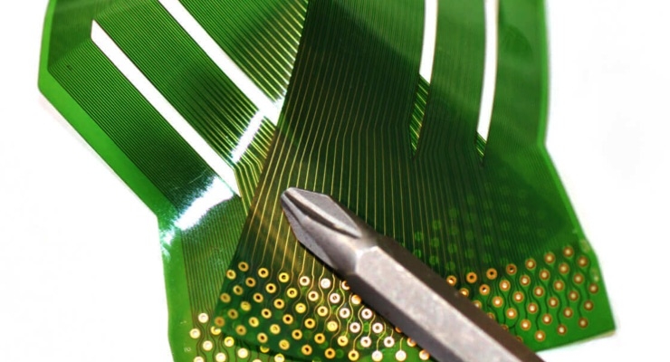
This Flex PCB is thin and light has intricate laser slots and copper “bumps.’ (Source: MicroConnex)
A specialist in commercial flexible circuits fabrication and laser micromachining services, Snoqualmie, WA-based MicroConnex develops high-density flex interconnects (HDI) solutions for the electronic packaging market. The company uses its proprietary photolithographic patterning systems to produce custom flexible circuitry. Key markets include medical ultrasound systems, semiconductor and defense and aerospace industries.
Steve Leith, MicroConnex’s VP engineering and technology, said that MicroConnex was formed as an R&D company called MicroSound Systems in the mid-1990s.
“The initial business concept was to develop next generation, complex medical ultrasound transducers and this early work were partially funded by DARPA and the US Navy,” Leith said. “The company co-founders were experts in ultrasound, but during the course of the project found that the 2D ultrasonic transducers required complex interconnects not readily available from third parties. By necessity they had to develop high-density flex interconnects (HDI) in-house to enable demonstration of the ultrasonic device.
“In developing the skill in fabricating specialty flex circuits, it became clear that the real value proposition of the company wasn’t ultrasonic devices, but fabricating the interconnects required to interface with the mesoscale world,” he added. “The team then created MicroConnex as a technology-centric business focused on high-density flex circuit fabrication leveraging the company expertise in laser micro-machining and thin film deposition.”
The HDI business is highly competitive. MicroConnex is working with the Washington Clean Energy Test Beds (WCET) to overcome the cost vs. performance pressure in the HDI marketplace.
“We believe that we can address a portion of the market needs using a hybrid circuit fabrication process that utilizes elements of printing and electrodeposition; our colleagues at WCET are experts in printing on plastic technology and MicroConnex has a very deep bench in electrodeposition of nano- and micro-scale architectures,” Leith noted. “The idea to combine these two technologies resulted from an assessment of circuit functional requirements vs. available, reasonably mature fabrication processes.”
Leith said that ideal markets for MicroConnex are those that require the smallest and thinnest densely populated flexible circuitry.
“Examples abound in the medical device space in which small and thin circuit design elements are required for functionality,” he reported. “Specifically, electrophysiology (EP) mapping/ablation applications (i.e. cardiac mapping and ablation) are platforms that benefit from HDI circuit technology. Hearing aids (including cochlear implants), vision enhancement devices, drug delivery, and medical ultrasound are other applications in which HDI plays a key role. The motivation for the technology under development is that flex circuits made with the hybrid process may be used to fabrication these types of devices with disruptive performance vs cost metrics.”
One of the biggest challenges has been the ability to use roll-to-roll fabrication techniques. NextFlex is funding MicroConnex’s project to develop a two-step “hybrid” printing process in which fine circuit patterns are first printed using an R2R process.
“In the last 10-15 years, significant resources (people and R&D funds) have been spent trying to solve some fundamental material and processing challenges in R2R printed electronics fabrication,” said Leith. “The technology has evolved and improved based on hard work and wide-ranging contributions by numerous industrial and academic developers around the globe, yet many of the same issues remain. The primary technical challenges include demonstrating adequate adhesion of the printed material to the substrate (does the circuit stick to the plastic), achieving targeted dimensional control of the circuits (how accurately circuit widths and thickness can be controlled) and fabricating circuits with sufficient electrical performance to be useful (primarily high enough conductivity).
“Adhesion is influenced by the chemical and physical attributes of the substrate, the chemical and physical attributes of the printed ‘ink’ that becomes the circuit and the specific process used in ‘rolling’ the ink onto the substrate (think pressure, speed, temperature, roller material, etc.),” Leith continued. “We are working with our colleagues at WCET to evaluate the interactions and results of using different inks, different substrates and a range of clean and ink application processes to identify optimized print conditions for adhesion.”
Leith noted that many of the same substrate, ink and R2R process attributes that impact adhesion also play a role in the ability to control the circuit dimensions.
“We use a similar experimental approach to evaluate optimum process conditions for printing circuits of different dimensions as described above; i.e. we are exploring a range of ink formulations, substrates and application methods to identify which process combinations can be used to fabricate circuits of certain dimensions. Again, our colleagues at WCET are leaders in this field and are driving the experimental plan and execution,” he said.
“Printing circuits with acceptable adhesion and controlled dimensions is not new and a large body of work exists upon which we are expanding our understanding. Printing very narrow circuits in a high-density design, however, remains super challenging and is a primary focus of our work,” Leith added.
In order to improve conductivity, MicroConnex and WCET are using a hybrid production process.
“The R2R process is being “tuned” to create narrow circuits in high-density designs,” Leith said. “The downside is that after the first step (printing), the circuits are typically poor conductors and have low electrical functionality. The second step in the hybrid process is designed to add additional, high conductivity metal to the circuit printed in step one. This additional metal increases the conductivity of the circuit to acceptable levels without compromising the dimensions or adhesion of the originally printed trace. The result of the hybrid process is a circuit that achieves a commercially viable combination of small dimensions, good adhesion and acceptable electrical properties.
“When successful, the proposed hybrid circuit fabrication process will not only enable MicroConnex to increase revenue, but the R2R process should be lower cost, ultimately leading to higher profit margins and/or lower pricing for our medical customers,” Leith concluded.
Leith sees NextFlex as being an ideal partner in developing a manufacturing ecosystem, adding that the funded project will demonstrate production volume capability and commercial viability.
“We face unrelenting pricing pressure from lower-cost labor markets, especially in the volume production segment of our business,” said Leith. “In the big picture, we see investments in technology and automation as a key element in maintaining our competitive advantage in both performance and pricing. The NextFlex-funded project is one example of how the domestic PCB/FHE sector, in general, can spend resources to create and maintain a high tech industrial manufacturing base in the US. Without the funding from NextFlex, a company of our size likely wouldn’t be able to invest the resources to tackle such a risky and expensive R&D project.”
This Flex PCB is thin and light has intricate laser slots and copper “bumps.’ (Source: MicroConnex)