08.07.18
OLED microdisplays are increasingly establishing themselves in consumer-ready wearables and data glasses. In order to meet the requirements for higher efficiency, higher contrast, and higher resolutions in these applications, Fraunhofer FEP scientists have developed a new micropatterning approach for OLEDs on silicon substrates.
This might eliminate the use of color filters and shadow masks in the future and allow full-color displays to be developed by means of a new process. An increase in efficiency and considerably broader color gamut have already been demonstrated in first experiments. The results will be presented at the Fraunhofer FEP booth and during the poster session at IMID 2018 in Busan, South Korea, Aug. 29-31, 2018.
The average smartphone user looks at a display about 88 times a day, not counting viewing smaller smart watches or other displays. Displays of all kinds have become ubiquitous and will soon be irreplaceable in everyday life.
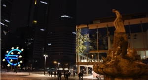
In addition to industrial use in Production 4.0 programs and products, its use in medical technology and in electronic entertainment, AR and VR applications have also been established for years in advertising and the education sector. The days of bulky audio guides in museums could soon be over, and not only as a result of previous solutions like tablets and smartphones. Lightweight head-up displays can turn exhibitions into learning worlds by integrating film scenes, audio, and interaction with the visitor to make a museum experience more memorable.
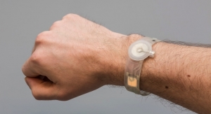
Due to the shallow overall depth that results from the self-luminous properties of OLEDs and their excellent contrast ratios, manufacturers are increasingly turning to OLED microdisplays for AR/VR glasses. Fraunhofer FEP has been continuously immersed in the advanced development of this technology for several years. There are still some technological challenges that need to be mastered in order to reach the full potential of OLED technology for use in consumer-ready data glasses and other AR/VR applications. Very high brightness and efficiency, good yields for large chip areas, curved surfaces, integrated eye tracking, and transparent substrates are some of the tasks still on the researchers’ agenda.
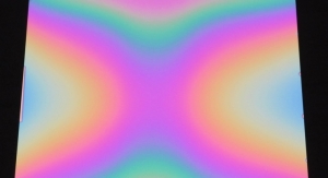
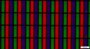
Currently, OLED technology faces the hurdle that full-color displays can only be realized by using color filters or shadow masks, which limit OLED efficiency and resolution. The patterning of the organic layers of OLEDs is one of the greatest challenges since conventional methods such as photolithography cannot be utilized with organic semiconductor materials.
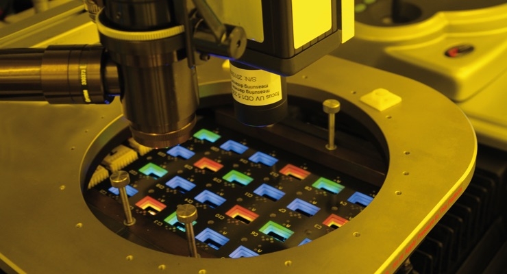
The use of electron beam technology for microstructuring was successfully demonstrated at the Fraunhofer FEP two years ago. Using its patented process, FEP was able to modify the emission of an OLED through the existing encapsulation layer to create any feature imaginable and even produce high-resolution grayscale images.
Further development of the electron beam process has now achieved full-color OLED without using color filters or shadow masks. To create red, green, and blue pixels, an organic layer of the OLED itself is ablated by a thermal electron beam process. This patterning causes a change to the thickness of the layer stack, which makes the emission of different colors possible. This is the first major step towards the development of full-color displays without the use of restrictive color filters in the process.
“With our electron-beam process it is possible to thermally structure even these sensitive organic materials without damaging the underlying layer,” noted Elisabeth Bodenstein, developer in the Fraunhofer FEP project team.
In addition to using this new process for OLEDs, electron beam processing can also be used for other applications in organic electronics and inorganic layers. The electron-beam patterning process is adaptable and can also be employed in the areas of photovoltaics, MEMS and thin-film technology. The next step planned is to integrate the micropatterning into existing processes in order to gain further know-how jointly with industrial partners.
Source: Fraunhofer FEP.
This might eliminate the use of color filters and shadow masks in the future and allow full-color displays to be developed by means of a new process. An increase in efficiency and considerably broader color gamut have already been demonstrated in first experiments. The results will be presented at the Fraunhofer FEP booth and during the poster session at IMID 2018 in Busan, South Korea, Aug. 29-31, 2018.
The average smartphone user looks at a display about 88 times a day, not counting viewing smaller smart watches or other displays. Displays of all kinds have become ubiquitous and will soon be irreplaceable in everyday life.
In addition to industrial use in Production 4.0 programs and products, its use in medical technology and in electronic entertainment, AR and VR applications have also been established for years in advertising and the education sector. The days of bulky audio guides in museums could soon be over, and not only as a result of previous solutions like tablets and smartphones. Lightweight head-up displays can turn exhibitions into learning worlds by integrating film scenes, audio, and interaction with the visitor to make a museum experience more memorable.
Due to the shallow overall depth that results from the self-luminous properties of OLEDs and their excellent contrast ratios, manufacturers are increasingly turning to OLED microdisplays for AR/VR glasses. Fraunhofer FEP has been continuously immersed in the advanced development of this technology for several years. There are still some technological challenges that need to be mastered in order to reach the full potential of OLED technology for use in consumer-ready data glasses and other AR/VR applications. Very high brightness and efficiency, good yields for large chip areas, curved surfaces, integrated eye tracking, and transparent substrates are some of the tasks still on the researchers’ agenda.
Currently, OLED technology faces the hurdle that full-color displays can only be realized by using color filters or shadow masks, which limit OLED efficiency and resolution. The patterning of the organic layers of OLEDs is one of the greatest challenges since conventional methods such as photolithography cannot be utilized with organic semiconductor materials.
The use of electron beam technology for microstructuring was successfully demonstrated at the Fraunhofer FEP two years ago. Using its patented process, FEP was able to modify the emission of an OLED through the existing encapsulation layer to create any feature imaginable and even produce high-resolution grayscale images.
Further development of the electron beam process has now achieved full-color OLED without using color filters or shadow masks. To create red, green, and blue pixels, an organic layer of the OLED itself is ablated by a thermal electron beam process. This patterning causes a change to the thickness of the layer stack, which makes the emission of different colors possible. This is the first major step towards the development of full-color displays without the use of restrictive color filters in the process.
“With our electron-beam process it is possible to thermally structure even these sensitive organic materials without damaging the underlying layer,” noted Elisabeth Bodenstein, developer in the Fraunhofer FEP project team.
In addition to using this new process for OLEDs, electron beam processing can also be used for other applications in organic electronics and inorganic layers. The electron-beam patterning process is adaptable and can also be employed in the areas of photovoltaics, MEMS and thin-film technology. The next step planned is to integrate the micropatterning into existing processes in order to gain further know-how jointly with industrial partners.
Source: Fraunhofer FEP.