07.10.19
Applied Materials, Inc. unveiled high-volume manufacturing solutions aimed at accelerating industry adoption of new memory technologies targeting the Internet of Things (IoT) and cloud computing.
Today’s high-volume memory technologies including DRAM, SRAM and flash were invented decades ago and have become ubiquitous in digital devices and systems. New memories – notably MRAM, ReRAM and PCRAM – promise unique benefits, but they are based on new materials that have been too challenging for high-volume manufacturing.
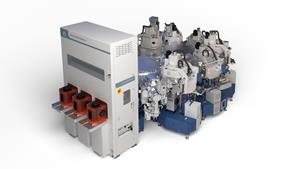
Applied Materials is introducing new manufacturing systems that allow novel materials – the key to these new memories – to be deposited with atomic-level precision. The company is delivering the most advanced systems it has ever developed to enable these promising new memories to be reliably produced at an industrial scale.
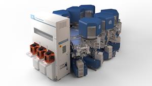
“The new Endura platforms we are introducing today are the most sophisticated chip-making systems our company has ever created,” said Dr. Prabu Raja, SVP and GM of Applied’s semiconductor products group. “Our broad portfolio gives us the unique ability to integrate multiple materials engineering technologies along with onboard metrology to create new films and structures that were not possible until now. These integrated platforms illustrate the critical role that new materials and 3D architectures can play in giving the computing industry entirely new ways to improve performance, power and cost.”
“IBM has been spearheading R&D of new memories for many years, and we see the need for these technologies increasing as the AI era demands improvements in chip performance and efficiency,” said Mukesh Khare, VP, semiconductors, AI Hardware and Systems, IBM Research. “New materials and device types can play an important role in enabling high-performance, low-power embedded memory for IoT, Cloud and AI products. Applied Materials’ high-volume manufacturing solutions can help accelerate the availability of these new memories across the industry.”