Kerry Pianoforte, Coatings World Editor03.24.17
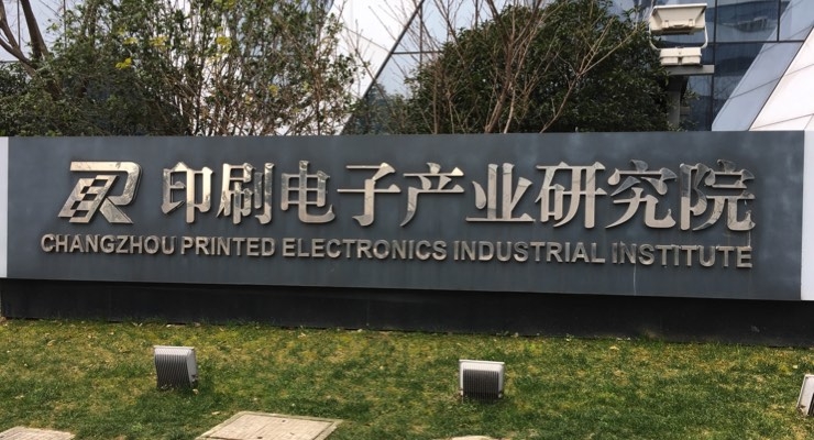
The Changzhou Institute of Printed Electronics Industry (IPEI) was established in September 2013. It is the first R&D facility to address printed electronics commercialization needs. In addition to developing PE core technologies for industry applications, IPEI provides services through the PE value chain for technology incubation. IPEI works with scientists, start-up companies, OEMs and investors from all over the world who are dedicated to PE technology commercialization.
IPEI has six platforms for printed electronics commercialization:
• Modularized multiple-stage R2R production lines with integrated printing/coatings/assembly technologies.
• Fully equipped functional test and analytical center.
• China PE Public Service Platform authorized by the national government based on big data processing and cloud services.
• R&D laboratory.
• Printed electronics exhibition and education center.
• Printed electronics standardization center.
IPEI’s new pilot facility will be completed in May 2017. The new modern facility will feature an integrated pilot line - the Multiple Stage R2R System features printing speeds up to 50m/min, web width of 350 mm, registration between stages of 0.05 mm, high tolerance for selecting flexible substrates, in-line thermal and UV curing/sintering capabilities and modularized system for fast change-over and reconfiguring printing line.
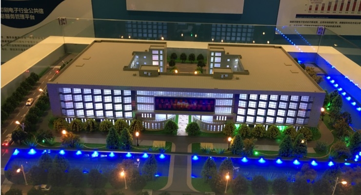
The Printed Electronics Industrial Park will be equipped with multiple stage/function R2R end-to-end manufacturing lines; capable for Class 10,00 cleanroom operation; feature full function and reliability test labs from materials, devices and products and have lab and office space for incubation.
To date IPEI has launched a number of products including paper-thin flexible primary battery, RFID enabled smart temperature tag for cold-chain management and flexible temperature sensors for the heath care industry. IPEI welcomes collaborations co-developing PE core technologies, prototyping R&D technology for potential applications, materials and process scale-up for manufacturing, printed and flexible electronics production R&D and printed and flexible electronics contract manufacturing.
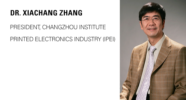
The IPEI is led by its president, Xiachang Zhang, PhD, whose expertise is in printed thin film battery technology, supply chain management, health care products and market development. Jie Zhang, PhD, is VP, and her areas of expertise are in printed and flexible electronics, optoelectronics materials, devices, processes and applications.
Recently, Printed Electronics Now visited IPEI, and had the opportunity to interview Dr. Zhang
PEN: What is the mission of the Changzhou Institute of Printed Electronics Industry?
Dr. Zhang: The Institute is committed to the industrialization of printed electronics in China. To this aim, it has been building several platforms to provide facilitation services, including: R & D on the technology of industrialization, commercialization of scientific and technological achievements, industrial technology transfer, production scale-up, standardization, and venture capital financing, among others.
PEN: What have been some of the most important developments by the Institute since it opened in 2013?
Dr. Zhang: First, public platform construction. The Institute has been promoting the construction of six public platforms. We have completed the construction of the China Printed Electronics Industry Public Service Platform, the integrated pilot platform, and the technology and physical product display platform, and nearing completion was the construction of the standards & certification sub-center, the public laboratory, and the public testing center. These platforms will provide all-around support for the industrialization of printed electronics technology in China.
Second, project incubation. We have been incubating start-ups by launching printed electronics industrialization projects. Up till now, three start-ups have been successfully incubated, and one of them has gained equity investment from a listed company, which has laid the foundation for its large-scale entry into the market.
Third, team building. A complete R & D and industrialization team has been established, led by seven top scientists including Dr. Zhang Xiachang, father of the paper battery, and Dr. Zhang Jie, a world-class expert on printing electronics.
Fourth, international cooperation. Cooperative ties have been established with several leading international organizations in the field of printed electronics, such as the Centre for Process Innovation (CPI), the Organic and Printed Electronics Association (OE-A), and the Agency for Science, Technology and Research (A*STAR), and IDTechEx.
Fifth, conference organization. We have organized 3 printed electronics industry conferences. In particular, we held The Sixth Chinese Flexible And Printed Electronic Symposium & The First International FPE Industry Summit in October 2016, which attracted the participation of a record-high number of guests and audience, including Klaus Hecker (CEO of OE-A), Raghu Das (CEO of IDTechEX), and leaders from the Chinese Ministry of Industry and Information Technology.
PEN: The Chinese government sees many possibilities for the printed electronics field. How is the government of China supporting the Institute?
Dr. Zhang: The Chinese government recognizes that the printed electronic technology is a golden opportunity for China to transform itself from “Made in China” to “Created in China.” In this spirit, it has been providing substantial support to the Institute in the following aspects: a. government resources are used to serve the docking between the upstream and downstream industrialization; b. efforts have been underway to build the world’s first printed electronics industry park, with the first phase of the project covering a building area of 60,000 square meters and integrating into one such functions as administration, R & D, experiment, and production; c. a number of talent introduction policies have been made, and meanwhile support has been given for the Institute to expand exchanges and cooperation by organizing international industry conferences; d. a printing electronics industry fund has been set up in collaboration with social capital; and e. enormous funds have been invested into the Institute’s undergoing construction of six platforms, including the pilot platform and mass production lines, public laboratories, and testing centers. The Chinese government has included the printing display technology in its 13th Five-Year Plan for national scientific and technological innovation, which will be advanced as a national key R & D plan. This is a huge support at the national strategic level.
PEN: What do you see as the fastest growing markets for printed electronics?
Dr. Zhang: The printed electronics market owes its rapid development to the fleetingly rising demand in emerging consumer electronics in recent years, especially in areas of Internet of Things, wearable electronic devices and health monitoring. Though already very mature and even saturated, the traditional electronics industry cannot effectively meet demands of the emerging consumer market for thin, flexible, portable, discardable, and pollution-free electronic products.
In comparison, the printed electronics technology, which is a new green manufacturing technology for creating electronics on flexible substrates, has the advantages of less material consumption, lower cost, zero pollution, softness, lighter weight, and thinness. Thus, printed electronics is the perfect match for the demands and trends of the emerging consumer electronics market. With the gradual popularization of printed electronics as well as the increasing participation of specialists in the market, we are full of confidence in the future market — there must be a major breakthrough in the industrialization of printed electronics in five years, and man will not be able to go without the printed electronics technology in their daily life in 10 years. Printed electronics, which is based on green manufacturing, will become an indispensable part in the world’s advanced intelligent manufacturing.
PEN: What will be some of the capabilities (personnel, equipment) that the Institute will have?
Dr. Zhang: Committed to the industrialization of the printed electronics technology, the Institute will acquire the following abilities: a. R & D capacities necessary for continuous optimization of functional materials and the printed electronics technology; b. marketing abilities to turn technologies into products and quickly popularize products in the customer market; and c. servicing and organizing abilities to incubate start-ups, apply for research projects, and organize industry conferences.
Meanwhile, it will be staffed with a world-leading research and manufacturing team composed of specialists in all aspects of printed and flexible electronics: a. researchers on the R & D and preparation of functional materials; b. application architects and designers; c. senior engineers skillful at scaling up production processes; d. senior technicians and developers familiar with printing processes (i.e., screenprinting, dispensing, spray coating, letterpress and gravure, etc.) and integrated processes. e. quality controllers familiar with quality standards, testing methods, and testing standards for conventional electronic devices; f. market personnel with long experience in market development and feedbacks on product improvement needs of electronic products and related applications; and g. administrative support staff responsible to bring in and incubate start-ups, apply for all kinds of science and technology projects, and hold industry conferences.
In term of technical ability, the Institute will boast core technologies and patents on printed flexible paper batteries, printed integrated circuits, cold chain logistics labels, and medical care sensors. When it comes to equipment, the Institute will be equipped with an integrated pilot production facility which is based on the roll-to-roll printing technology and has a maximum production capacity of 1B units / year, coupled with experiment and testing equipment for analysis and testing of various materials, performance testing for electronic products, and reliability verification.
PEN: What will the capabilities of the new pilot facility, and how will it help the Chinese industry?
Dr. Zhang: As the world’s first integrated pilot facility for printed electronics, the pilot facility boasts first-rate performances in the industry, in terms of printing accuracy, production speed, and product diversity, representing an excellent example of the Institution’s authority and representativeness as a world-leading institution of its kind.
The pilot facility will facilitate the industrialization of printed electronics in three directions. First, it can provide a platform for public testing and pilot production and verification, so as to bring mature printed electronics technologies or products from laboratories to mass production. Second, it can form a flexible hybrid electronic system by effectively combining the printed electronics technology and microelectronic components, with an aim to developing more applications and accelerating the industrialization in this regard. Third, it can help start-ups go through difficulties in early production, in an effort to resolve their urgent problem of funding shortage in early stages and thereby promote industrialization.
PEN: Who are some of the largest companies in printed electronics in China?
Dr. Zhang: In pace with the global development, the printed electronics technology has been accepted by a wide range of industries in China, such as electronics, optoelectronics, health care, and logistics management. Now, several large enterprises, including Huawei, TCL and Invengo Information Technology Co., Ltd., have been involved in the R & D and application of the printed electronic technology.
Additionally, there have emerged many innovative enterprises on printed electronics, including Changzhou Printed Electronics Co., Ltd. (in addition to its core products — paper batteries, its product portfolio also includes a wide range of applications, such as wearable electronic products, monitoring devices for IoT-based logistics, and intelligent packaging); Beijing Nano Top Electronic Technology Co., Ltd. (an affiliated enterprise under Institute of Chemistry, Chinese Academy of Sciences, which mainly specializes in the R & D and production of conductive silver paste, packaging adhesives, and nano-silver conductive films), Suzhou Leanstar Electronic Technology Co., Ltd. (an affiliated enterprise under Suzhou Institute of Nano Tech and Nano Bionics, Chinese Academy of Sciences, which mainly specializes in the R & D and production of electronic skin, MEMS silicon-based micro hot plates), and Shenzhen-based Royole Corp. (specializes in the R & D of flexible display, flexible sensing, VR display, and related smart devices), among others.
PEN: What do you see as the potential for printed electronics in China and globally in the coming years?
Dr. Zhang: With the rapid development of the emerging consumer electronics market and the IT technology, as well as the ever-increasing improvement of printed electronics technology per se and corresponding preparation technology, industrialization of printed electronics will usher in a real outbreak period featuring rapid development in market segments of flexible OLED display and lighting, flexible intelligent integrated systems, flexible intelligence (sensor) tags, with the overall market value of the industry expected to reach hundreds of billions of US dollars.
Among all market segments, that of OLED display is expected to be the largest. In particular, the mass production of flexible OLED display products based on inkjet printing technology will contribute to an effective reduction of costs. Flexible OLED display, which can find large-scale application in mobile phones, tablet PCs, TVs, and other display terminals, is expected to occupy huge market shares.
The next is the market segment of flexible intelligent integrated systems based on environmentally friendly and efficient paper batteries, low-power chips, Internet of Things/Internet, and the cloud computing technology. Intelligent integrated systems are expected to be widely used for wearable medical health monitoring devices, wearable consumer electronics, tracking and monitoring of cold chain logistics, smart packaging, and other fields, with the market value expected to reach billions of dollars by 2020.
Given its huge development potential, the key path for the industrialization of printed electronics is to adopt hybrid systems. Specifically, mature microelectronic components will be combined partly with the printed electronics technology and integrated into flexible hybrid electronic products. In this way, not only can effective play be given into the advantages of printed electronics, but also there can be significant reduction of costs and a guarantee of product performance, so that enterprises can timely grasp the market opportunities by quickly popularizing printed electronics in the application areas. Taking into account its manufacturing capacity and huge market, China will act as a major promoter and sponsor in the worldwide industrialization of printed electronics.

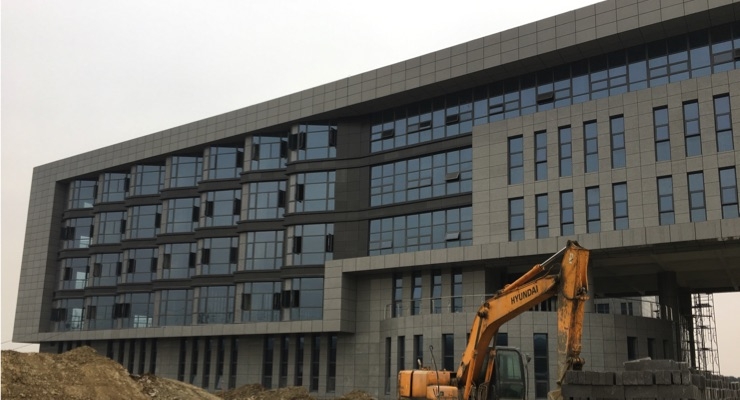
Construction is underway on IPEI's new pilot facility.
IPEI has six platforms for printed electronics commercialization:
• Modularized multiple-stage R2R production lines with integrated printing/coatings/assembly technologies.
• Fully equipped functional test and analytical center.
• China PE Public Service Platform authorized by the national government based on big data processing and cloud services.
• R&D laboratory.
• Printed electronics exhibition and education center.
• Printed electronics standardization center.
IPEI’s new pilot facility will be completed in May 2017. The new modern facility will feature an integrated pilot line - the Multiple Stage R2R System features printing speeds up to 50m/min, web width of 350 mm, registration between stages of 0.05 mm, high tolerance for selecting flexible substrates, in-line thermal and UV curing/sintering capabilities and modularized system for fast change-over and reconfiguring printing line.
The Printed Electronics Industrial Park will be equipped with multiple stage/function R2R end-to-end manufacturing lines; capable for Class 10,00 cleanroom operation; feature full function and reliability test labs from materials, devices and products and have lab and office space for incubation.
To date IPEI has launched a number of products including paper-thin flexible primary battery, RFID enabled smart temperature tag for cold-chain management and flexible temperature sensors for the heath care industry. IPEI welcomes collaborations co-developing PE core technologies, prototyping R&D technology for potential applications, materials and process scale-up for manufacturing, printed and flexible electronics production R&D and printed and flexible electronics contract manufacturing.
The IPEI is led by its president, Xiachang Zhang, PhD, whose expertise is in printed thin film battery technology, supply chain management, health care products and market development. Jie Zhang, PhD, is VP, and her areas of expertise are in printed and flexible electronics, optoelectronics materials, devices, processes and applications.
Recently, Printed Electronics Now visited IPEI, and had the opportunity to interview Dr. Zhang
PEN: What is the mission of the Changzhou Institute of Printed Electronics Industry?
Dr. Zhang: The Institute is committed to the industrialization of printed electronics in China. To this aim, it has been building several platforms to provide facilitation services, including: R & D on the technology of industrialization, commercialization of scientific and technological achievements, industrial technology transfer, production scale-up, standardization, and venture capital financing, among others.
PEN: What have been some of the most important developments by the Institute since it opened in 2013?
Dr. Zhang: First, public platform construction. The Institute has been promoting the construction of six public platforms. We have completed the construction of the China Printed Electronics Industry Public Service Platform, the integrated pilot platform, and the technology and physical product display platform, and nearing completion was the construction of the standards & certification sub-center, the public laboratory, and the public testing center. These platforms will provide all-around support for the industrialization of printed electronics technology in China.
Second, project incubation. We have been incubating start-ups by launching printed electronics industrialization projects. Up till now, three start-ups have been successfully incubated, and one of them has gained equity investment from a listed company, which has laid the foundation for its large-scale entry into the market.
Third, team building. A complete R & D and industrialization team has been established, led by seven top scientists including Dr. Zhang Xiachang, father of the paper battery, and Dr. Zhang Jie, a world-class expert on printing electronics.
Fourth, international cooperation. Cooperative ties have been established with several leading international organizations in the field of printed electronics, such as the Centre for Process Innovation (CPI), the Organic and Printed Electronics Association (OE-A), and the Agency for Science, Technology and Research (A*STAR), and IDTechEx.
Fifth, conference organization. We have organized 3 printed electronics industry conferences. In particular, we held The Sixth Chinese Flexible And Printed Electronic Symposium & The First International FPE Industry Summit in October 2016, which attracted the participation of a record-high number of guests and audience, including Klaus Hecker (CEO of OE-A), Raghu Das (CEO of IDTechEX), and leaders from the Chinese Ministry of Industry and Information Technology.
PEN: The Chinese government sees many possibilities for the printed electronics field. How is the government of China supporting the Institute?
Dr. Zhang: The Chinese government recognizes that the printed electronic technology is a golden opportunity for China to transform itself from “Made in China” to “Created in China.” In this spirit, it has been providing substantial support to the Institute in the following aspects: a. government resources are used to serve the docking between the upstream and downstream industrialization; b. efforts have been underway to build the world’s first printed electronics industry park, with the first phase of the project covering a building area of 60,000 square meters and integrating into one such functions as administration, R & D, experiment, and production; c. a number of talent introduction policies have been made, and meanwhile support has been given for the Institute to expand exchanges and cooperation by organizing international industry conferences; d. a printing electronics industry fund has been set up in collaboration with social capital; and e. enormous funds have been invested into the Institute’s undergoing construction of six platforms, including the pilot platform and mass production lines, public laboratories, and testing centers. The Chinese government has included the printing display technology in its 13th Five-Year Plan for national scientific and technological innovation, which will be advanced as a national key R & D plan. This is a huge support at the national strategic level.
PEN: What do you see as the fastest growing markets for printed electronics?
Dr. Zhang: The printed electronics market owes its rapid development to the fleetingly rising demand in emerging consumer electronics in recent years, especially in areas of Internet of Things, wearable electronic devices and health monitoring. Though already very mature and even saturated, the traditional electronics industry cannot effectively meet demands of the emerging consumer market for thin, flexible, portable, discardable, and pollution-free electronic products.
In comparison, the printed electronics technology, which is a new green manufacturing technology for creating electronics on flexible substrates, has the advantages of less material consumption, lower cost, zero pollution, softness, lighter weight, and thinness. Thus, printed electronics is the perfect match for the demands and trends of the emerging consumer electronics market. With the gradual popularization of printed electronics as well as the increasing participation of specialists in the market, we are full of confidence in the future market — there must be a major breakthrough in the industrialization of printed electronics in five years, and man will not be able to go without the printed electronics technology in their daily life in 10 years. Printed electronics, which is based on green manufacturing, will become an indispensable part in the world’s advanced intelligent manufacturing.
PEN: What will be some of the capabilities (personnel, equipment) that the Institute will have?
Dr. Zhang: Committed to the industrialization of the printed electronics technology, the Institute will acquire the following abilities: a. R & D capacities necessary for continuous optimization of functional materials and the printed electronics technology; b. marketing abilities to turn technologies into products and quickly popularize products in the customer market; and c. servicing and organizing abilities to incubate start-ups, apply for research projects, and organize industry conferences.
Meanwhile, it will be staffed with a world-leading research and manufacturing team composed of specialists in all aspects of printed and flexible electronics: a. researchers on the R & D and preparation of functional materials; b. application architects and designers; c. senior engineers skillful at scaling up production processes; d. senior technicians and developers familiar with printing processes (i.e., screenprinting, dispensing, spray coating, letterpress and gravure, etc.) and integrated processes. e. quality controllers familiar with quality standards, testing methods, and testing standards for conventional electronic devices; f. market personnel with long experience in market development and feedbacks on product improvement needs of electronic products and related applications; and g. administrative support staff responsible to bring in and incubate start-ups, apply for all kinds of science and technology projects, and hold industry conferences.
In term of technical ability, the Institute will boast core technologies and patents on printed flexible paper batteries, printed integrated circuits, cold chain logistics labels, and medical care sensors. When it comes to equipment, the Institute will be equipped with an integrated pilot production facility which is based on the roll-to-roll printing technology and has a maximum production capacity of 1B units / year, coupled with experiment and testing equipment for analysis and testing of various materials, performance testing for electronic products, and reliability verification.
PEN: What will the capabilities of the new pilot facility, and how will it help the Chinese industry?
Dr. Zhang: As the world’s first integrated pilot facility for printed electronics, the pilot facility boasts first-rate performances in the industry, in terms of printing accuracy, production speed, and product diversity, representing an excellent example of the Institution’s authority and representativeness as a world-leading institution of its kind.
The pilot facility will facilitate the industrialization of printed electronics in three directions. First, it can provide a platform for public testing and pilot production and verification, so as to bring mature printed electronics technologies or products from laboratories to mass production. Second, it can form a flexible hybrid electronic system by effectively combining the printed electronics technology and microelectronic components, with an aim to developing more applications and accelerating the industrialization in this regard. Third, it can help start-ups go through difficulties in early production, in an effort to resolve their urgent problem of funding shortage in early stages and thereby promote industrialization.
PEN: Who are some of the largest companies in printed electronics in China?
Dr. Zhang: In pace with the global development, the printed electronics technology has been accepted by a wide range of industries in China, such as electronics, optoelectronics, health care, and logistics management. Now, several large enterprises, including Huawei, TCL and Invengo Information Technology Co., Ltd., have been involved in the R & D and application of the printed electronic technology.
Additionally, there have emerged many innovative enterprises on printed electronics, including Changzhou Printed Electronics Co., Ltd. (in addition to its core products — paper batteries, its product portfolio also includes a wide range of applications, such as wearable electronic products, monitoring devices for IoT-based logistics, and intelligent packaging); Beijing Nano Top Electronic Technology Co., Ltd. (an affiliated enterprise under Institute of Chemistry, Chinese Academy of Sciences, which mainly specializes in the R & D and production of conductive silver paste, packaging adhesives, and nano-silver conductive films), Suzhou Leanstar Electronic Technology Co., Ltd. (an affiliated enterprise under Suzhou Institute of Nano Tech and Nano Bionics, Chinese Academy of Sciences, which mainly specializes in the R & D and production of electronic skin, MEMS silicon-based micro hot plates), and Shenzhen-based Royole Corp. (specializes in the R & D of flexible display, flexible sensing, VR display, and related smart devices), among others.
PEN: What do you see as the potential for printed electronics in China and globally in the coming years?
Dr. Zhang: With the rapid development of the emerging consumer electronics market and the IT technology, as well as the ever-increasing improvement of printed electronics technology per se and corresponding preparation technology, industrialization of printed electronics will usher in a real outbreak period featuring rapid development in market segments of flexible OLED display and lighting, flexible intelligent integrated systems, flexible intelligence (sensor) tags, with the overall market value of the industry expected to reach hundreds of billions of US dollars.
Among all market segments, that of OLED display is expected to be the largest. In particular, the mass production of flexible OLED display products based on inkjet printing technology will contribute to an effective reduction of costs. Flexible OLED display, which can find large-scale application in mobile phones, tablet PCs, TVs, and other display terminals, is expected to occupy huge market shares.
The next is the market segment of flexible intelligent integrated systems based on environmentally friendly and efficient paper batteries, low-power chips, Internet of Things/Internet, and the cloud computing technology. Intelligent integrated systems are expected to be widely used for wearable medical health monitoring devices, wearable consumer electronics, tracking and monitoring of cold chain logistics, smart packaging, and other fields, with the market value expected to reach billions of dollars by 2020.
Given its huge development potential, the key path for the industrialization of printed electronics is to adopt hybrid systems. Specifically, mature microelectronic components will be combined partly with the printed electronics technology and integrated into flexible hybrid electronic products. In this way, not only can effective play be given into the advantages of printed electronics, but also there can be significant reduction of costs and a guarantee of product performance, so that enterprises can timely grasp the market opportunities by quickly popularizing printed electronics in the application areas. Taking into account its manufacturing capacity and huge market, China will act as a major promoter and sponsor in the worldwide industrialization of printed electronics.
Construction is underway on IPEI's new pilot facility.