07.16.15
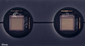
Imec and SPTS Technologies, an Orbotech company announced at SEMICON West that they are jointly developing a highly accurate, short cycle-time dry silicon removal and low temperature passivation solution for through-silicon via-middle processing and thinning of the top-wafer in wafer-to-wafer bonding.
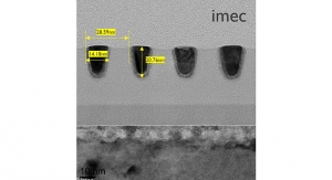
Wafer backside processing is critical for 3D-IC wafer stacking. Today, through-silicon vias (TSV) formed using ‘via-middle’ processing, are typically exposed from the backside of 300mm device wafers by a combination of mechanical grinding and wet or dry etch processes. Dielectric layers are then deposited by plasma enhanced chemical vapor deposition (PECVD) to passivate and mechanically support the exposed TSVs prior to bump/RDL (redistribution) formation, followed by chip-to-wafer or wafer-to-wafer bonding.
Imec and SPTS are developing a dry etching solution that features in-situ end-point detection. This enables controlled and very precise processing.
To follow the via reveal etch step, imec and SPTS will also work on PECVD dielectric passivation stacks, with SiO and SiN layers deposited at temperatures below 200°C.
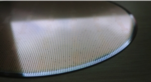
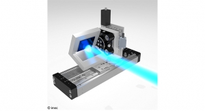
The collaboration will use SPTS’s Versalis fxP system, a single-wafer cluster platform carrying both etch and dielectric deposition modules to be installed into imec’s 300mm packaging line in Q3 2015.
Wafer backside processing is critical for 3D-IC wafer stacking. Today, through-silicon vias (TSV) formed using ‘via-middle’ processing, are typically exposed from the backside of 300mm device wafers by a combination of mechanical grinding and wet or dry etch processes. Dielectric layers are then deposited by plasma enhanced chemical vapor deposition (PECVD) to passivate and mechanically support the exposed TSVs prior to bump/RDL (redistribution) formation, followed by chip-to-wafer or wafer-to-wafer bonding.
Imec and SPTS are developing a dry etching solution that features in-situ end-point detection. This enables controlled and very precise processing.
To follow the via reveal etch step, imec and SPTS will also work on PECVD dielectric passivation stacks, with SiO and SiN layers deposited at temperatures below 200°C.
The collaboration will use SPTS’s Versalis fxP system, a single-wafer cluster platform carrying both etch and dielectric deposition modules to be installed into imec’s 300mm packaging line in Q3 2015.